Diodes DMN6066SSD User Manual

A
f
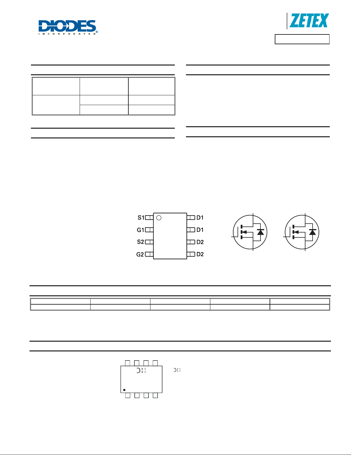
Product Summary
V
R
(BR)DSS
60V
DS(on)
66mΩ @ V
97mΩ @ VGS = 4.5V
GS
= 10V
Description and Applications
This MOSFET has been designed to minimize the on-state resistance
and yet maintain superior switching performance, making it ideal for
high efficiency power management applications.
• Motor control
ADVANCE INFORMATION
• Backlighting
• DC-DC Converters
• Power management functions
SO-8
Top View
T
= 25°C
A
4.4A
3.6A
Product Line o
Diodes Incorporated
DMN6066SSD
60V DUAL N-CHANNEL ENHANCEMENT MODE MOSFET
Features and Benefits
I
D
• Low on-resistance
• Fast switching speed
• 100% Unclamped Inductive Switch (UIS) test in production
• “Green” component and RoHS compliant (Note 1)
• Qualified to AEC-Q101 Standards for High Reliability
Mechanical Data
• Case: SO-8
• Case Material: Molded Plastic, “Green” Molding Compound. UL
Flammability Classification Rating 94V-0 (Note 1)
• Moisture Sensitivity: Level 1 per J-STD-020
• Terminals Connections: See diagram below
• Terminals: Finish - Matte Tin annealed over Copper lead frame.
Solderable per MIL-STD-202, Method 208
• Weight: 0.074 grams (approximate)
D2
S2
Top View
G1
D1
G2
S1
Equivalent Circuit
Ordering Information (Note 1)
Product Marking Reel size (inches) Tape width (mm) Quantity per reel
DMN6066SSD-13 N6066SD 13 12 2,500
Note: 1. Diodes, Inc. defines “Green” products as those which are RoHS compliant and contain no halogens or antimony compounds; further information about
Diodes Inc.’s “Green” Policy can be found on our website. For packaging details, go to our website.
Marking Information
DMN6066SSD
Document Number DS32109 Rev 3 - 2
N6066SD
YY
WW
= Manufacturer’s Marking
N6066SD = Product Type Marking Code
YYWW = Date Code Marking
YY = Year (ex: 09 = 2009)
WW = Week (01 - 53)
www.diodes.com
1 of 9
December 2011
© Diodes Incorporated

A
f
A
A
θ
Product Line o
Diodes Incorporated
DMN6066SSD
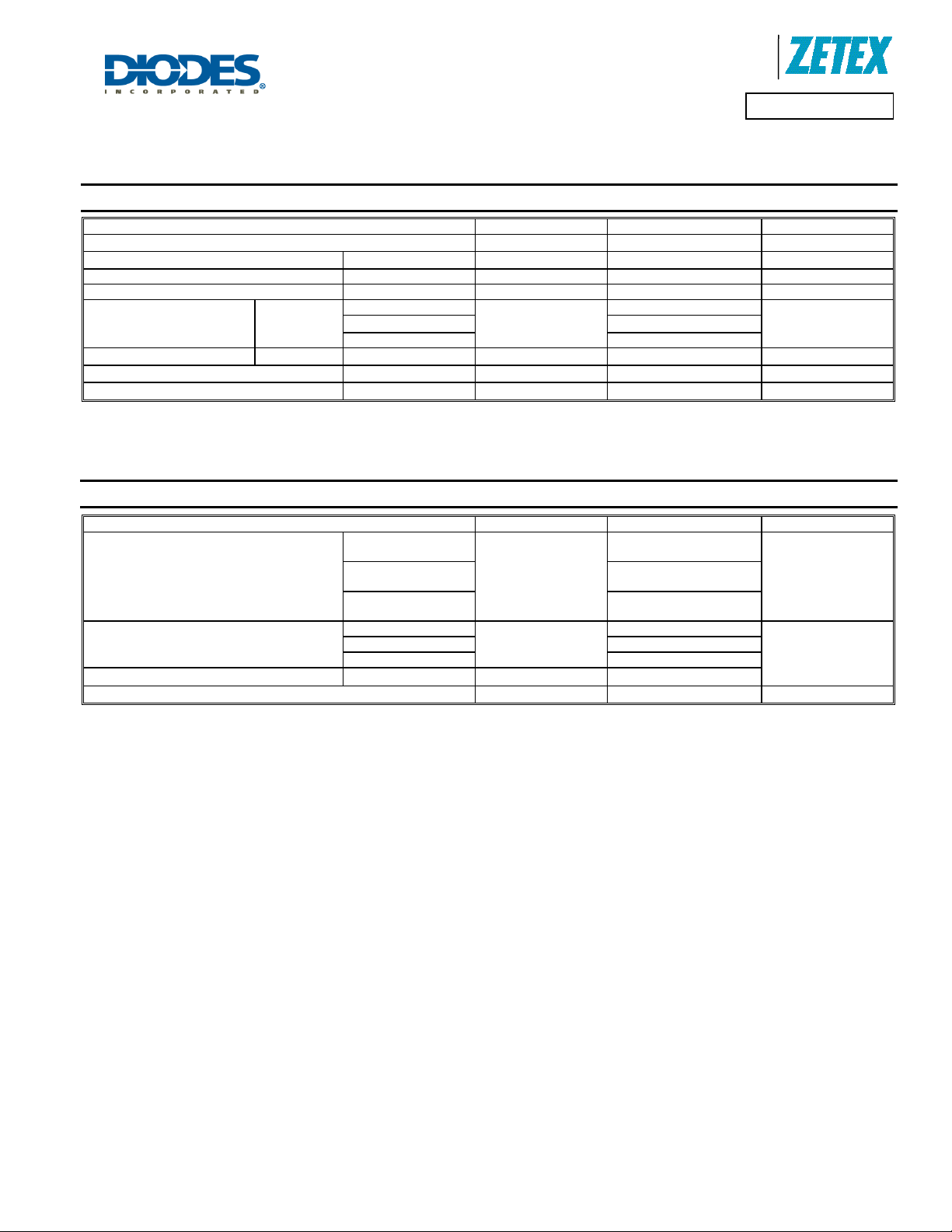
Maximum Ratings @T
= 25°C unless otherwise specified
A
Characteristic Symbol Value Unit
Drain-Source voltage
Gate-Source voltage (Note 2)
Single Pulsed Avalanche Energy (Note 9) E
Single Pulsed Avalanche Current (Note 9) I
(Note 4)
Continuous Drain current
V
GS
= 10V
TA = 70°C (Note 4)
(Note 3) 3.3
Pulsed Drain current
V
GS
= 10V
(Note 5)
Continuous Source current (Body diode) (Note 4)
Pulsed Source current (Body diode) (Note 5)
ADVANCE INFORMATION
Thermal Characteristics @T
= 25°C unless otherwise specified
A
Characteristic Symbol Value Unit
(Notes 3 & 6)
Power dissipation
Linear derating factor
(Notes 3 & 7)
(Notes 4 & 6)
(Notes 3 & 6)
Thermal Resistance, Junction to Ambient
(Notes 3 & 7) 70
(Notes 4 & 6) 58
Thermal Resistance, Junction to Lead (Notes 6 & 8)
Operating and storage temperature range
Notes: 2. AEC-Q101 VGS maximum is ±16V.
measured when operating in a steady-state condition.
3. For a device surface mounted on 25mm x 25mm x 1.6mm FR4 PCB with high coverage of single sided 1oz copper, in still air conditions; the device is
4. Same as note (3), except the device is measured at t ≤ 10 sec.
5. Same as note (3), except the device is pulsed with D = 0.02 and pulse width 300µs. The pulse current is limited by the maximum junction temperature.
6. For a dual device with one active die.
7. For a device with two active die running at equal power.
8. Thermal resistance from junction to solder-point (at the end of the drain lead).
9. UIS in production with L = 3.0mH, I
= 5.0A, RG = 25, VDD = 50V, starting TJ = 25°C.
AS
V
DSS
V
GS
37.5 mJ
S
5.0 A
S
60 V
±20
V
4.4
I
D
IDM
I
S
I
SM
3.5
17.0 A
3.2 A
17.0 A
A
1.25
10
P
D
1.8
14.3
W
mW/°C
2.14
17.2
100
R
JA
θ
R
JL
T
, T
J
STG
55
-55 to 150
°C/W
°C
DMN6066SSD
Document Number DS32109 Rev 3 - 2
2 of 9
www.diodes.com
December 2011
© Diodes Incorporated

A
f
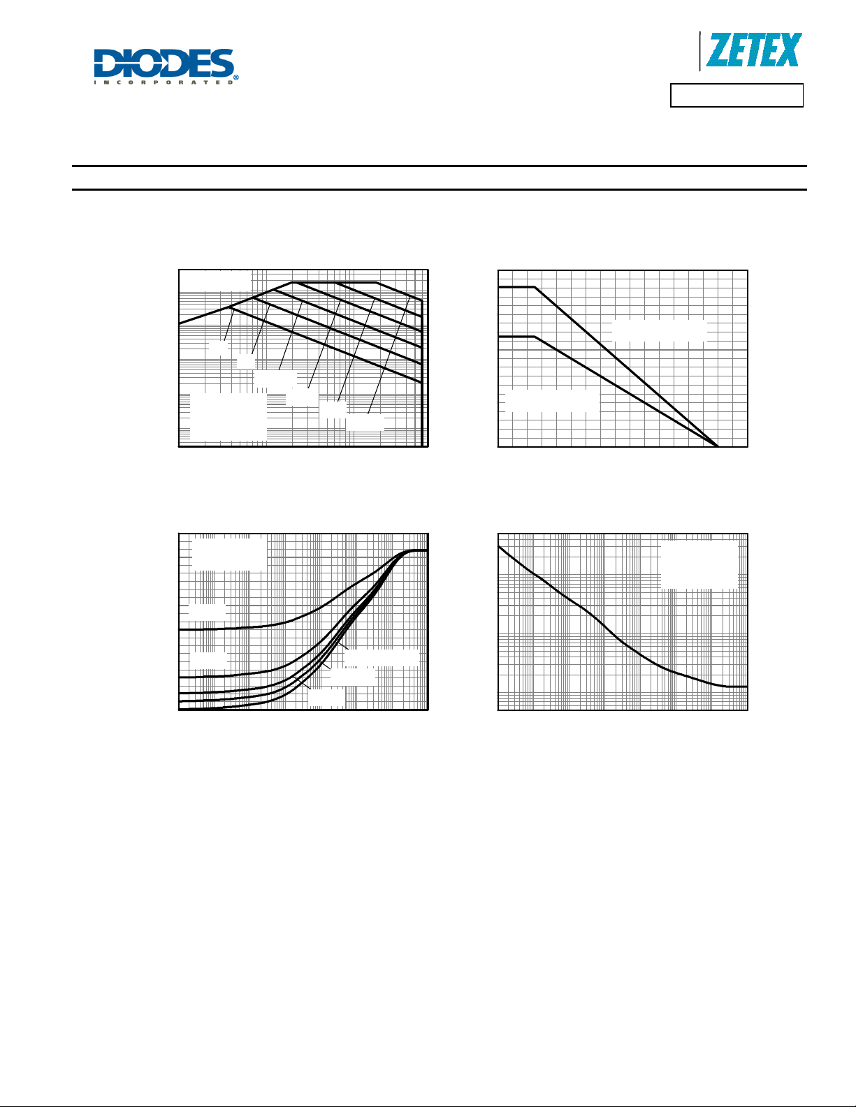
Thermal Characteristics
Product Line o
Diodes Incorporated
DMN6066SSD
R
Limited
DS(on)
10
1
100m
10m
ADVANCE INFORMATION
Drain Current (A)
1m
D
I
100m 1 10
DC
1s
Single Pulse
T
=25°C
amb
One active die
100ms
10ms
1ms
100µs
VDS Drain-Source Voltage (V)
Safe Operating Area
110
100
90
80
70
60
50
40
30
20
10
Thermal Resistance (°C/W)
T
=25°C
amb
One active die
D=0.5
D=0.2
0
100µ 1m 10m 100m 1 10 100 1k
Single Pulse
D=0.05
D=0.1
Pulse Width (s)
Transient Thermal Imp edan ce
2.0
1.8
1.6
1.4
1.2
1.0
0.8
0.6
One active die
0.4
0.2
0.0
0 20 40 60 80 100 120 140 160
Max Pow er D issipati o n (W )
Temperature (°C)
Two active die
Derating Curve
Single Pulse
T
=25°C
100
10
1
Maximum Power (W)
100µ 1m 10m 100m 1 10 100 1k
amb
One active die
Pulse Width (s)
Pulse Power Dissipation
DMN6066SSD
Document Number DS32109 Rev 3 - 2
3 of 9
www.diodes.com
December 2011
© Diodes Incorporated
 Loading...