Diodes DMN6040SVT User Manual

DMN6040SVT
60V N-CHANNEL ENHANCEMENT MODE MOSFET
Product Summary
I
V
(BR)DSS
60V
R
DS(on) max
44mΩ @ V
60mΩ @ VGS = 4.5V
= 10V
GS
D
TA = 25°C
5.0A
4.3A
Description and Applications
This new generation MOSFET has been designed to minimize the onstate resistance (R
performance, making it ideal for high efficiency power management
applications.
• DC-DC Converters
• Power management functions
• Backlighting
ADVANCE INFORMATION
) and yet maintain superior switching
DS(on)
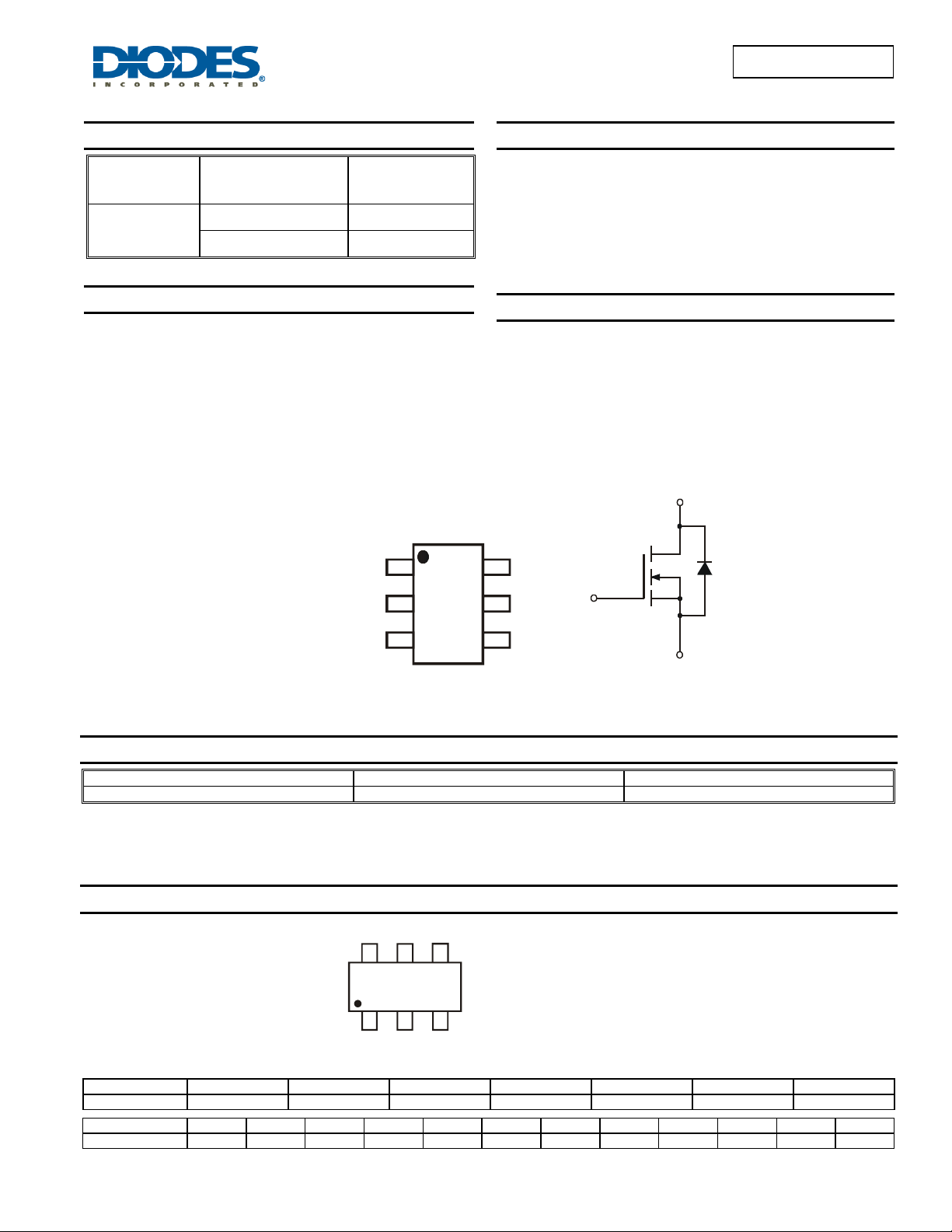
TSOT26
Top View Top View
D
1
D
2
3
G
Pin Configuration
Features and Benefits
• 100% Unclamped Inductive Switch (UIS) test in production
• Low Input Capacitance
• Low On-Resistance
• Fast Switching Speed
• Lead, Halogen, and Antimony Free, RoHS Compliant (Note 1)
• "Green" Device (Note 2)
• Qualified to AEC-Q101 Standards for High Reliability
Mechanical Data
• Case: TSOT26
• Case Material: Molded Plastic, “Green” Molding Compound.
UL Flammability Classification Rating 94V-0
• Moisture Sensitivity: Level 1 per J-STD-020
• Terminal Connections: See Diagram
• Terminals: Finish – Tin Finish annealed over Copper leadframe.
Solderable per MIL-STD-202, Method 208
• Weight: 0.013 grams (approximate)
Drain
Source
Body
Diode
D
6
Gate
D
5
4
S
Equivalent Circuit
Ordering Information (Note 3)
Part Number Case Packaging
DMN6040SVT-7 TSOT26 3,000/Tape & Reel
Notes: 1. EU Directive 2002/95/EC (RoHS) & 2011/65/EU (RoHS 2) compliant. No purposely added lead. Halogen and Antimony free.
2. Diodes Inc.’s “Green” policy can be found on our website at http://www.diodes.com.
3. For packaging details, go to our website at http://www.diodes.com.
Marking Information
32D
32D = Product Type Marking Code
YM = Date Code Marking
YM
Y = Year (ex: X = 2010)
M = Month (ex: 9 = September)
Date Code Key
Year 2010 2011 2012 2013 2014 2015 2016
Code X Y Z A B C D
Month Jan Feb Mar Apr May Jun Jul Aug Sep Oct Nov Dec
Code 1 2 3 4 5 6 7 8 9 O N D
DMN6040SVT
Document number: DS35562 Rev. 10 - 2
1 of 7
www.diodes.com
March 2012
© Diodes Incorporated

θ
P, P
T
R
T P
O
R
RAIN C
URR
N
T
DMN6040SVT
Maximum Ratings @T
= 25°C unless otherwise specified
A
Characteristic Symbol Value Units
Drain-Source Voltage
Gate-Source Voltage
Continuous Drain Current (Note 5) VGS = 10V
Continuous Drain Current (Note 5) VGS = 5V
Maximum Body Diode Forward Current (Note 5)
Pulsed Drain Current (10μs pulse, duty cycle = 1%)
Avalanche Current (Note 6) L = 0.1mH
Avalanche Energy (Note 6) L = 0.1mH
Steady
State
t<10s
Steady
State
t<10s
T
= 25°C
A
T
= 70°C
A
= 25°C
T
A
= 70°C
T
A
T
= 25°C
A
T
= 70°C
A
= 25°C
T
A
= 70°C
T
A
V
DSS
V
GSS
I
D
I
D
I
D
I
D
I
S
I
DM
I
AR
E
AR
60 V
±20 V
5.0
4.0
6.3
5.0
4.3
3.4
5.4
4.3
A
A
A
A
2.1 A
30 A
14.2 A
10 mJ
ADVANCE INFORMATION
Thermal Characteristics @T
Total Power Dissipation (Note 4)
Thermal Resistance, Junction to Ambient (Note 4)
Total Power Dissipation (Note 5)
Thermal Resistance, Junction to Ambient (Note 5)
Thermal Resistance, Junction to Case (Note 5)
Operating and Storage Temperature Range
100
= 25°C unless otherwise specified
A
Characteristic Symbol Value Units
= 25°C
T
A
TA = 70°C
Steady state
t<10s 69 °C/W
T
= 25°C
A
TA = 70°C
Steady state
t<10s 44 °C/W
P
R
P
R
R
T
J, TSTG
D
JA
θ
D
JA
θ
JC
1.2
0.75
W
106 °C/W
1.8
1.1
W
68 °C/W
20 °C/W
-55 to +150 °C
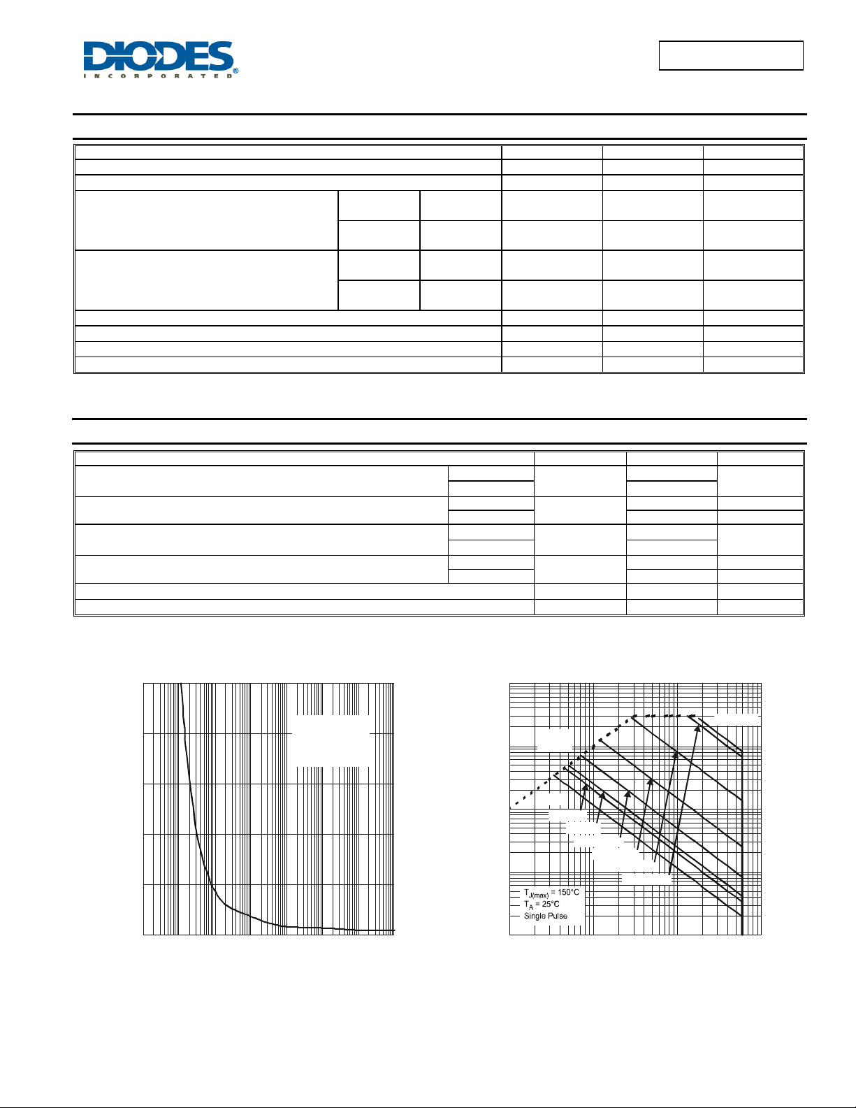
100
Single Pulse
(W)
80
IWE
R = 72C/W
θ
JA
R = r * R
θθ
JA(t) (t) JA
T - T = P * R
JA JA(t)
60
ANSIEN
40
EAK
20
(PK)
0
0.001 0.01 0.1 1 10 100 1,0000.0001
t1, PULSE DURATION TIME (sec)
Fig. 1 Single Pulse Maximum Power Dissipation
°
10
θ
(A)
R
DS(on)
Limited
E
DC
P = 10s
W
P = 1s
W
P = 100ms
W
P = 10ms
W
P = 1ms
W
P = 100µs
W
D
I, D
1
0.1
0.01
0.1 1 10 100
V , DRAIN-SOURCE VOLT AGE (V)
DS
Fig. 2 SOA, Safe Operation Area
P = 10sWµ
DMN6040SVT
Document number: DS35562 Rev. 10 - 2
2 of 7
www.diodes.com
March 2012
© Diodes Incorporated

T
R
T T
HER
R
T
C
)
g
g
g
g
)
r
)
r
r
DMN6040SVT
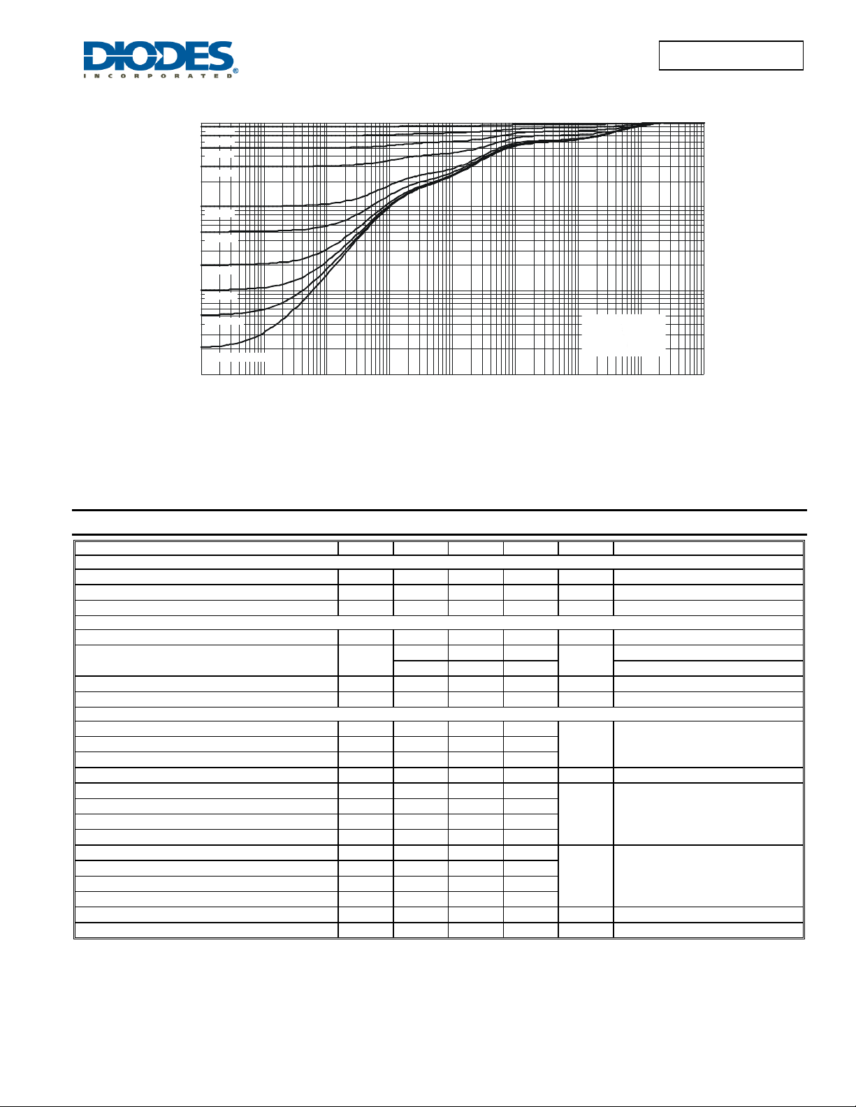
1
D = 0.9
D = 0.7
E
D = 0.5
AN
D = 0.3
ESIS
0.1
D = 0.1
MAL
D = 0.05
D = 0.02
0.01
D = 0.01
ANSIEN
D = 0.005
r(t),
D = Single Pulse
0.001
0.00001 0.0001 0.001 0.01 0.1 1 10 100 1,000
R = r * R
θ
JA(t) (t)
R = 72C/W
JA
Duty Cycle, D = t1/t2
θθJA
°
t1, PULSE DURATION TIME (sec)
Fig. 3 Transi ent Thermal Resistance
ADVANCE INFORMATION
Electrical Characteristics @T
= 25°C unless otherwise specified
A
Characteristic Symbol Min Typ Max Unit Test Condition
OFF CHARACTERISTICS (Note 7)
Drain-Source Breakdown Voltage
Zero Gate Voltage Drain Current
Gate-Source Leakage
BV
I
DSS
I
GSS
DSS
60
⎯ ⎯
⎯ ⎯
⎯ ⎯
V
100 nA
±100
nA
VGS = 0V, ID = 250μA
VDS = 60V, VGS = 0V
V
= ±20V, VDS = 0V
GS
ON CHARACTERISTICS (Note 7)
Gate Threshold Voltage
Static Drain-Source On-Resistance
Forward Transfer Admittance
Diode Forward Voltage
V
GS(th
R
DS (ON)
|Y
V
SD
| ⎯
fs
1
⎯
⎯
⎯
⎯
30 44
35 60
4.5
0.7 1.2 V
3 V
⎯
VDS = VGS, ID = 250μA
V
mΩ
VGS = 4.5V, ID = 4A
S
V
VGS = 0V, IS = 1A
= 10V, ID = 4.3A
GS
= 10V, ID = 4.3A
DS
DYNAMIC CHARACTERISTICS (Note 8)
Input Capacitance
Output Capacitance
Reverse Transfer Capacitance
Gate Resistance
Total Gate Charge (VGS = 10V)
Total Gate Charge (VGS = 4.5V)
Gate-Source Charge
Gate-Drain Charge
Turn-On Delay Time
Turn-On Rise Time
Turn-Off Delay Time
Turn-Off Fall Time
Body Diode Reverse Recovery Time
Body Diode Reverse Recovery Charge
Notes: 4. Device mounted on FR-4 substrate PC board, 2oz copper, with minimum recommended pad layout.
5. Device mounted on FR-4 substrate PC board, 2oz copper, with 1inch square copper plate.
6. I
and EAR rating are based on low frequency and duty cycles to keep TJ = 25°C
AR
7. Short duration pulse test used to minimize self-heating effect.
8. Guaranteed by design. Not subject to product testing.
C
C
C
Q
Q
t
D(on
t
D(off
iss
oss
rss
R
G
Q
Q
s
d
t
t
f
t
r
Q
r
⎯
⎯
⎯
⎯
⎯
⎯
⎯
⎯
⎯
⎯
⎯
⎯
⎯
⎯
1287
57
44
1.2
22.4
10.4
4.9
3.0
6.6
8.1
20.1
4.0
18
11.9
⎯
⎯
pF
⎯
⎯ Ω
⎯
⎯
⎯
nC
⎯
⎯
⎯
⎯
nS
⎯
⎯
⎯
nS
nC
V
= 25V, VGS = 0V
DS
f = 1.0MHz
VDS = 0V, VGS = 0V, f = 1.0MHz
V
= 30V, ID = 4.3A
DS
V
= 10V, VDD = 30V, RG = 6Ω,
GS
I
= 4.3A
D
IS = 4.3A, dI/dt = 100A/μs
IS = 4.3A, dI/dt = 100A/μs
DMN6040SVT
Document number: DS35562 Rev. 10 - 2
3 of 7
www.diodes.com
March 2012
© Diodes Incorporated
 Loading...