

Page 1
θ
)
)
)
r
N-CHANNEL ENHANCEMENT MODE FIELD EFFECT TRANSISTOR
Features
• Low On-Resistance
• Ideal for Notebook Computer, Portable Phone, PCMCIA
Cards, and Battery Power Circuits
• Lead Free By Design/RoHS Compliant (Note 2)
• Qualified to AEC-Q101 Standards for High Reliability
• ESD Protected Gate
• "Green" Device (Note 3)
Mechanical Data
• Case: SC59
• Case Material - Molded Plastic, “Green” Molding
Compound. UL Flammability Classification Rating 94V-0
• Moisture Sensitivity: Level 1 per J-STD-020C
• Terminals: Finish – Matte Tin annealed over Copper
leadframe. Solderable per MIL-STD-202, Method 208
• Terminal Connections: See Diagram
• Marking Information: See Page 3
• Ordering & Date Code Information: See Page 3
• Weight: 0.014 grams (approximate)
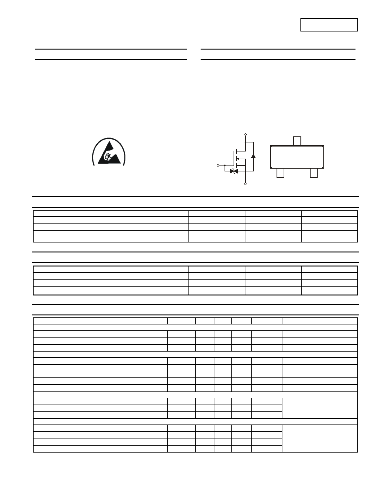
SC-59
Drain
NEW PRODUCT
ESD protected
TOP VIEW
Maximum Ratings @T
Drain-Source Voltage
Gate-Source Voltage Continuous
Drain Current Continuous
Pulsed
= 25°C unless otherwise specified
A
Characteristic Symbol Value Unit
Gate
Gate
Protection
Diode
Internal Schematic
V
DSS
V
GSS
ID
Source
20 V
±12
1.2
4.0
G
TOP VIEW
DMN2114SN
D
S
V
A
Thermal Characteristics @T
= 25°C unless otherwise specified
A
Characteristic Symbol Value Unit
Total Power Dissipation
Thermal Resistance, Junction to Ambient
Operating and Storage Temperature Range
R
Tj, T
Pd
JA
STG
500 mW
250
-55 to +150
°C /W
°C
Electrical Characteristics @T
= 25°C unless otherwise specified
A
Characteristic Symbol Min Typ Max Unit Test Condition
OFF CHARACTERISTICS (Note 1)
Drain-Source Breakdown Voltage
Zero Gate Voltage Drain Current @ Tj = 25°C I
Gate-Body Leakage
BV
DSS
I
GSS
DSS
20
⎯ ⎯
⎯ ⎯
⎯ ⎯
V
10
μA
±10 μA
VGS = 0V, ID = 250μA
= 24V, VGS = 0V
V
DS
V
= ±12V, VDS = 0V
GS
ON CHARACTERISTICS (Note 1)
Gate Threshold Voltage
Static Drain-Source On-Resistance
Forward Transfer Admittance
Diode Forward Voltage
V
GS(th
R
DS (ON)
|Y
V
fs
SD
|
0.7
⎯ ⎯ ⎯
⎯
⎯
1.40 V
⎯
0.100
0.160
⎯
3.3
0.8 1.1 V
⎯
V
DS
V
Ω
S
GS
V
GS
VDS = 10V, ID = 0.5A
V
GS
= 10V, ID = 1.0mA
= 4.5V, ID = 0.5A
= 2.5V, ID = 0.5A
= 0V, IS = 1.0A
DYNAMIC CHARACTERISTICS
Input Capacitance
Output Capacitance
Reverse Transfer Capacitance
C
⎯
iss
C
⎯
oss
C
⎯
rss
180
120
45
⎯
⎯
⎯
pF
pF
pF
= 10V, VGS = 0V,
V
DS
= 1.0MHz
f
SWITCHING CHARACTERISTICS
Turn-On Delay Time
Turn-Off Delay Time
Turn-On Rise Time
Turn-Off Fall Time
Notes: 1. Pulse width ≤300μS, duty cycle ≤2%.
2. No purposefully added lead.
3. Diodes Inc's "Green" policy can be found on our website at http://www.diodes.com/products/lead_free/index.php.
DMN2114SN
Document number: DS30829 Rev. 5 - 2
t
⎯
D(ON
t
⎯
D(OFF
t
⎯
t
⎯
f
1 of 4
www.diodes.com
10
50
15
45
⎯
⎯
⎯
⎯
ns
ns
ns
ns
V
= 10V, ID = 0.5A,
DD
= 5.0V, R
V
GS
= 50Ω
GEN
August 2011
© Diodes Incorporated
Page 2
R
C
URRENT
RAIN CUR
REN
T
R
TATIC DRAIN-SOUR
C
NEW PRODUCT
DMN2114SN
5
T = 25°C
A
4
3V, 3.5V, 4V, 5V
3.5
4
V = 10V
DS
3
(A)
3
2.5V
3.0V
(A)
2.5
T = 125°C
A
2
2
AIN
D
I, D
1
0
0 0.5 1 1.5 2 2.5 3
V , DRAIN-SOURCE VOLTAGE (V)
DS
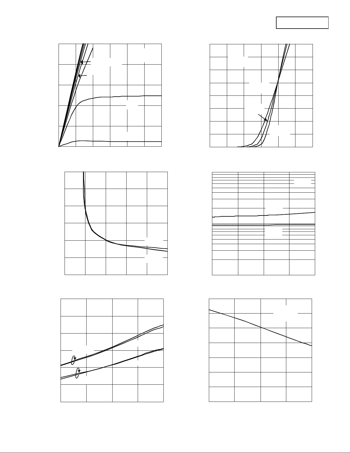
Fig. 1 Typical Output Character i st ics
0.3
0.25
E,
2.0V
V = 1.5V
GS
1.5
D
I, D
1
0.5
0
0 0.5 1 1.5 2 2.5 3
V , GA TE-SOURC E VOLTAGE (V)
GS
T= 25°C
A
T = -55°C
A
Fig. 2 Typical Transfer Characteristics
1
T = 25°C
J
, S
Ω
0.2
0.15
0.1
ON-RESISTNACE ( )
DS(ON)
0.05
0
0246810
V , GA TE-SOURC E VOLTAGE (V)
GS
I = 0.5A
D
I = 1.0A
D
Fig. 3 On- R esistance vs. Gate Voltage
0.3
Ω
0.25
0.2
RESISTANCE ( )
0.15
V = 2.5V
GS
I = 1.0A
D
I = 0.5A
D
Ω
2.5V
0.1
4.5V
ON-RESISTANCE ( )
DS(ON)
R , STATIC DRAIN-SOURCE,
0.01
01234
I , DRAIN CURRENT (A)
D
Fig. 4 On-R esista nc e vs. Drai n Cur r ent
1.4
V = 10V
1.2
DS
I = 1mA
D
1
0.8
0.6
I = 0.5A, 1A
0.1
D
0.4
V = 4.5V
0.05
0
-50 0 50 100 150
DS(ON)
R , STATIC DRAIN-SOURCE, ON-
Fig. 5 On-Resistance Variation with Temperature
GS
T , AMBIENT TEMPERATURE (°C)
A
0.2
GS(th)
V , GATE THRESHOLD VOLTAGE (V)
0
-50 0 50 100 150
T , AMBIENT TEMPERATURE (°C)
A
Fig. 6 Gat e Threshold Voltage vs. Temperatur e
DMN2114SN
Document number: DS30829 Rev. 5 - 2
2 of 4
www.diodes.com
August 2011
© Diodes Incorporated
Page 3

C, CAPAC
T
N
C
F
DMN2114SN
1,000
f = 1MHz
V = 0V
GS
T = 25°C
A
)
E (p
100
A
I
10
0 5 10 15 20
V , DRAIN-SOURCE VOLTAGE (V)
DS
C
iss
C
oss
C
rss
Fig. 8 Typical Total Capacitance
NEW PRODUCT
4
3.5
V = 4.5V
GS
3
2.5
2
1.5
1
0.5
0
0 0.2 0.4 0.6 0.8 1
V , SOURCE-DRAIN VOLTAGE (V)
Fig. 7 Reverse Drai n C ur r ent vs. Source-Drai n Voltage
SD
2.5V
0V -4.5V
Ordering Information (Note 4)
Part Number Case Packaging
DMN2114SN-7 SC59 3000/Tape & Reel
Notes: 4. For packaging details, go to our website at http://www.diodes.com/datasheets/ap02007.pdf.
Marking Information
NS2
NS2 = Product Type Marking Code
YM = Date Code Marking
YM
Y = Year ex: T = 2006
M = Month ex: 9 = September
Date Code Key
Year 2006 2007 2008 2009 2010 2011 2012
Code T U V W X Y Z
Month Jan Feb Mar Apr May Jun Jul Aug Sep Oct Nov Dec
Code 1 2 3 4 5 6 7 8 9 O N D
Package Outline Dimensions
DMN2114SN
Document number: DS30829 Rev. 5 - 2
K
J
A
TOP VIEW
G
H
D
Dim Min Max
SC59
A 0.35 0.50
C
B
B 1.50 1.70
C 2.70 3.00
D 0.95
E
⎯ ⎯
G 1.90
H 2.90 3.10
J 0.013 0.10
N
M
K 1.00 1.30
L 0.35 0.55
M 0.10 0.20
L
E
N 0.70 0.80
α
0° 8°
All Dimensions in mm
3 of 4
www.diodes.com
August 2011
© Diodes Incorporated
Page 4

DMN2114SN
Suggested Pad Layout
NEW PRODUCT
DIODES INCORPORATED MAKES NO WARRANTY OF ANY KIND, EXPRESS OR IMPLIED, WITH REGARDS TO THIS DOCUMENT,
INCLUDING, BUT NOT LIMITED TO, THE IMPLIED WARRANTIES OF MERCHANTABILITY AND FITNESS FOR A PARTICULAR PURPOSE
(AND THEIR EQUIVALENTS UNDER THE LAWS OF ANY JURISDICTION).
Diodes Incorporated and its subsidiaries reserve the right to make modifications, enhancements, improvements, corrections or other changes
without further notice to this document and any product described herein. Diodes Incorporated does not assume any liability arising out of the
application or use of this document or any product described herein; neither does Diodes Incorporated convey any license under its patent or
trademark rights, nor the rights of others. Any Customer or user of this document o r products described herein in such applica tions shall assume
all risks of such use and will agree to hold Diodes Incorporated and all the companies whose products are represented on Diodes Incorporated
website, harmless against all damages.
Diodes Incorporated does not warrant or accept any liability whatsoever in respect of any products purchased through unauthorized sales channel.
Should Customers purchase or use Diodes Incorporated products for any unintended or unauthorize d application, Customers shall indemnify and
hold Diodes Incorporated and its representatives harmless against all claims, damages, expenses, and attorney fees arising out of, directly or
indirectly, any claim of personal injury or death associated with such unintended or unauthorized application.
Products described herein may be covered by one or more United States, international or foreign patents pending. Product names and markings
noted herein may also be covered by one or more United States, international or foreign trademarks.
Diodes Incorporated products are specifically not authorized for use as critical components in life support devices or systems without the express
written approval of the Chief Executive Officer of Diodes Incorporated. As used herein:
A. Life support devices or systems are devices or systems which:
1. are intended to implant into the body, or
labeling can be reasonably expected to result in significant injury to the user.
B. A critical component is any component in a life support device or system whose failure to perform can be reasonably expected to cause the
failure of the life support device or to affect its safety or effectiveness.
Customers represent that they have all necessary expertise in the safety and regulatory ramifications of their life support devices or systems, and
acknowledge and agree that they are solely responsible for all legal, regulatory and safety-related requirements concerning their products and any
use of Diodes Incorporated products in such safety-critical, life support devices or systems, notwithstanding any devices- or systems-related
information or support that may be provided by Diodes Incorporated. Further, Customers must fully indemnify Diodes Incorporated and its
representatives against any damages arising out of the use of Diodes Incorporated products in such safety-critical, life support devices or systems.
Copyright © 2011, Diodes Incorporated
www.diodes.com
2. support or sustain life and whose failure to perform when properly used in accordance with instructions for use provided in the
Y
Z
G
C
X E
IMPORTANT NOTICE
LIFE SUPPORT
Dimensions Value (in mm)
Z 4.0
G 1.2
X 0.9
Y 1.4
C 2.6
E 0.95
DMN2114SN
Document number: DS30829 Rev. 5 - 2
4 of 4
www.diodes.com
August 2011
© Diodes Incorporated
 Loading...