

Page 1
θ
Features
• Low On-Resistance
• 8mΩ @ V
• 9mΩ @ V
• 12mΩ @ V
• Low Gate Threshold Voltage
• Low Input Capacitance
• Fast Switching Speed
• Low Input/Output Leakage
• Lead Free By Design/RoHS Compliant (Note 2)
• "Green" Device (Note 4)
• Qualified to AEC-Q101 Standards for High Reliability
= 10V
GS
= 4.5V
GS
GS
= 2.5V
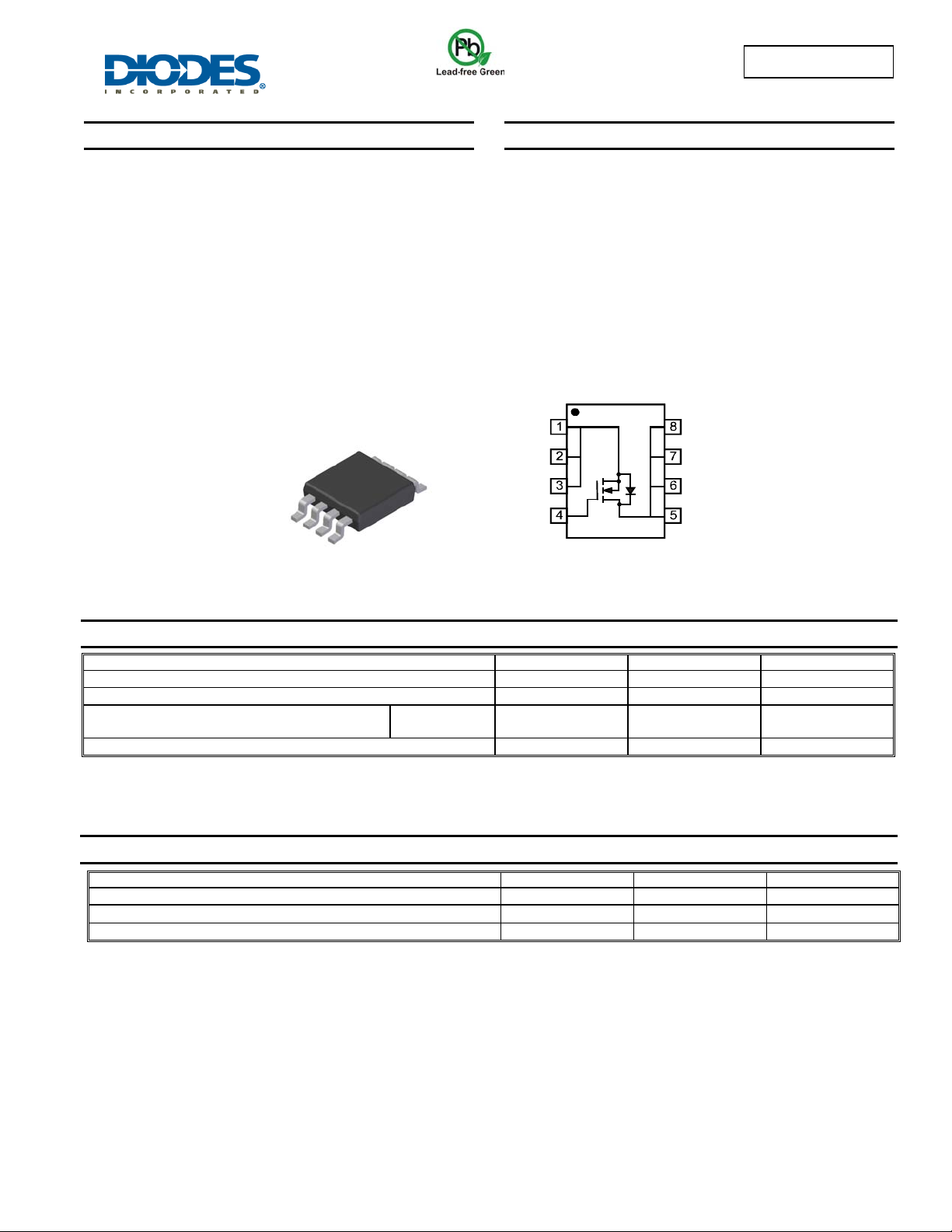
SO-8
TOP VIEW
DMN2009LSS
SINGLE N-CHANNEL ENHANCEMENT MODE MOSFET
Mechanical Data
• Case: SO-8
• Case Material: Molded Plastic, “Green” Molding Compound.
UL Flammability Classification Rating 94V-0
• Moisture Sensitivity: Level 1 per J-STD-020
• Terminals Connections: See Diagram
• Terminals: Finish - Matte Tin annealed over Copper lead frame.
Solderable per MIL-STD-202, Method 208
• Marking Information: See Page 4
• Ordering Information: See Page 4
• Weight: 0.072 grams (approximate)
S
S
S
G
TOP VIEW
Internal Schematic
D
D
D
D
Maximum Ratings @T
= 25°C unless otherwise specified
A
Characteristic Symbol Value Units
Drain-Source Voltage
Gate-Source Voltage
Drain Current (Note 1) Steady
State
Pulsed Drain Current (Note 3)
T
= 25°C
A
= 70°C
T
A
V
DSS
V
GSS
I
D
I
DM
20 V
±12
12
9.6
V
A
42 A
Thermal Characteristics
Characteristic Symbol Value Unit
Total Power Dissipation (Note 1)
Thermal Resistance, Junction to Ambient
Operating and Storage Temperature Range
Notes: 1. Device mounted on 2 oz, FR-4 PCB, with R
2. No purposefully added lead.
3. Pulse width ≤10μS, Duty Cycle ≤1%.
4. Diodes Inc.'s "Green" policy can be found on our website at http://www.diodes.com/products/lead_free/index.php.
= 62.5°C/W
JA
θ
P
R
T
J, TSTG
D
JA
DMN2009LSS
Document number: DS31409 Rev. 6- 2
1 of 5
www.diodes.com
2 W
62.5 °C/W
-55 to +150 °C
June 2010
© Diodes Incorporated
Page 2
)
g
g
R
N C
U
R
R
N
T
RAIN
C
U
R
REN
T
Electrical Characteristics @T
= 25°C unless otherwise specified
A
Characteristic Symbol Min Typ Max Unit Test Condition
OFF CHARACTERISTICS (Note 5)
Drain-Source Breakdown Voltage
Zero Gate Voltage Drain Current
Gate-Source Leakage
BV
DSS
I
⎯ ⎯
DSS
I
⎯ ⎯
GSS
ON CHARACTERISTICS (Note 5)
Gate Threshold Voltage
Static Drain-Source On-Resistance
Forward Transconductance
Diode Forward Voltage (Note 5)
V
GS(th
R
DS (ON)
V
g
fs
SD
⎯
DYNAMIC CHARACTERISTICS
Input Capacitance
Output Capacitance
Reverse Transfer Capacitance
Gate Resistance
C
iss
C
oss
C
rss
R
G
SWITCHING CHARACTERISTICS
Total Gate Charge
Gate-Source Charge
Gate-Drain Charge
Notes: 5. Short duration pulse test used to minimize self-heating effect.
Q
g
Q
⎯
s
Q
⎯
d
30
V = 10V
GS
25
(A)
20
E
V = 4.5V
GS
V = 4.0V
GS
V = 3.0V
GS
V = 2.5V
GS
V = 5V
DS
15
20
⎯ ⎯
1
±100
0.5
⎯
⎯
⎯
⎯
⎯
27
1.2 V
8
9
12
⎯
0.5 0.7 1.2 V
⎯
⎯
⎯
⎯
⎯
2555
523
496
1.1
28.9
58.3
3.7
11.4
⎯
⎯
⎯
⎯ Ω
⎯
⎯ VDS = 10V, VGS = 10V, ID = 12A
⎯ VDS = 10V, VGS = 10V, ID = 12A
V
V
GS
μA
V
nA
mΩ
DS
V
GS
V
DS
V
GS
V
GS
V
GS
S
V
DS
VGS = 0V, IS = 3A
pF
pF
V
DS
pF
VGS = 0V VDS = 0V, f = 1MHz
V
DS
V
nC
DS
30
25
V = 10V
(A)
20
15
DS
DMN2009LSS
= 0V, ID = 250μA
= 20V, VGS = 0V
= ±12V, VDS = 0V
= VGS, ID = 250μA
= 10V, ID = 12A
= 4.5V, ID = 10A
= 2.5V, ID = 8A
= 5V, ID = 6.5A
= 10V, VGS = 0V, f = 1.0MHz
= 10V, VGS = 4.5V, ID = 12A
= 10V, VGS = 10V, ID = 12A
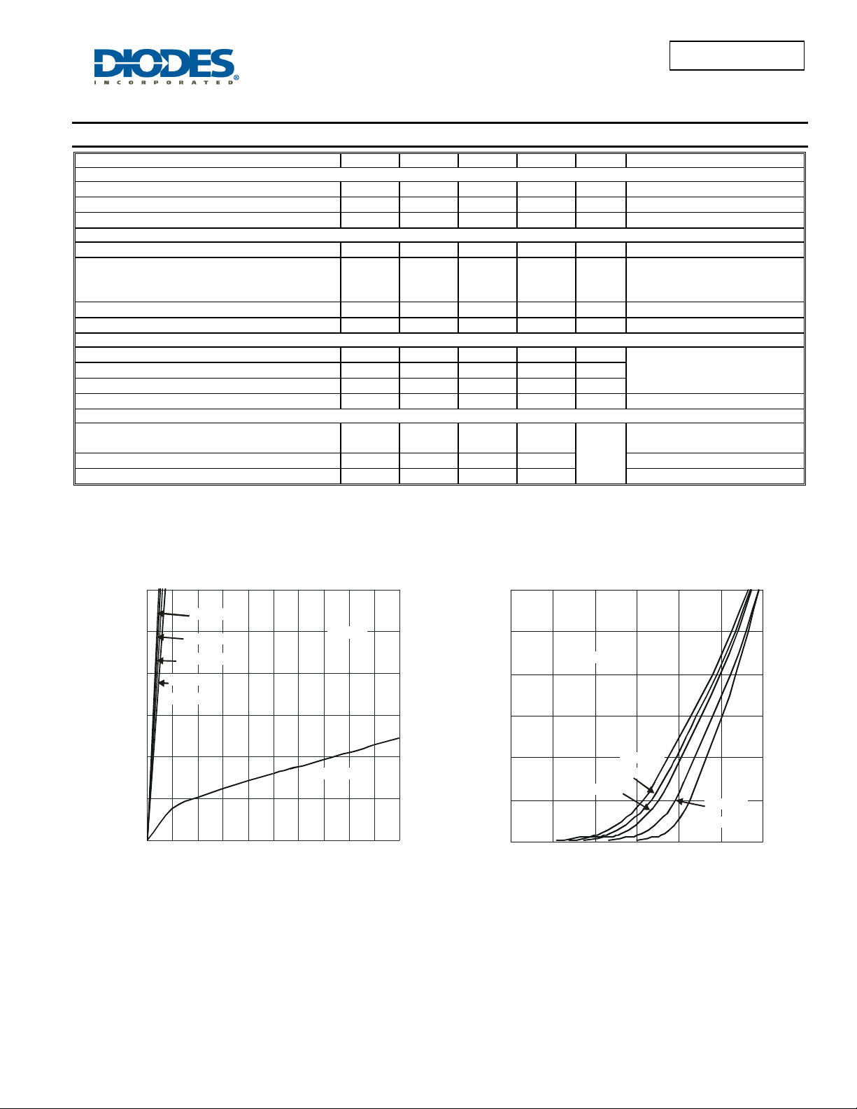
AI
D
I, D
10
V = 1.5V
GS
5
0
012345
V , DRAIN-SOURCE VOLT AGE (V)
DS
Fig. 1 Typical Output Characteristics
DMN2009LSS
Document number: DS31409 Rev. 6- 2
2 of 5
www.diodes.com
10
D
I, D
5
0
0.4 0.6 0.8 1 1.2 1.4 1.6
V , GATE SOURCE VOLTAGE (V)
GS
T = 150°C
T = 125°C
A
T = 85°C
A
A
T = 25°C
A
T = -55°C
A
Fig. 2 Typical Transfer Characteristics
June 2010
© Diodes Incorporated
Page 3
O
U
R
C
C
U
R
RENT
0.015
Ω
1.4
DMN2009LSS
1.3
V = 2.5V
GS
0.01
V = 4.5V
GS
I = 10A
D
I = 8A
V = 10V
I = 12A
0.005
DS(ON)
R , DRAIN-TO-SOURCE RESISTANCE ( )
0
-50 -25 0 25 50 75 100 125 150
T , AMBIENT TEMPERATURE (°C)
A
Fig. 3 On- Resistance Variation with Temperature
10,000
D
1.2
1.1
GS
D
DS(ON)
R , DRAIN-TO-SOURCE
1.0
RESISTANCE (NORMALIZED)
0.9
0.8
-50 -25 0 25 50 75 100 125 150
T , AMBIENT TEMPERATURE (°C)
A
Fig. 4 On-Resist ance Variation with T emperature
1.0
V = 4.5V
GS
I = 10A
D
V = 2.5V
GS
I = 8A
D
V = 10V
GS
I = 12A
D
C
iss
1,000
C
oss
C
C, CAPACITANCE (pF)
rss
100
048121620
V , DRAIN-SOURCE VOLTAGE (V)
DS
Fig. 5 Typical Capacitance
100
10
(A)
1
0.1
T = 150°C
T = 125°C
A
T = 85°C
A
A
E
T = 25°C
A
T = -55°C
A
S
I, S
0.01
0.001
0.8
I = 250µA
D
0.6
0.4
0.2
GS(TH)
V , GATE THRESHOLD VOL TAGE (V)
0
-50 -25 0 25 50 75 100 125 150
T , AMBIENT TEMPERATURE (°C)
A
Fig. 6 Gate Threshold Variation vs. Ambient Temperature
0.0001
0.1 0.2 0.3 0.4 0.5 0.6 0.7 0.8 0.9 1
V , SOURCE-DRAIN VOLTAGE (V)
SD
Fig. 7 Diode Forward Vol t age vs. Current
DMN2009LSS
Document number: DS31409 Rev. 6- 2
3 of 5
www.diodes.com
June 2010
© Diodes Incorporated
Page 4

T
R
T
T
HER
R
TANC
DMN2009LSS
1
E
D = 0.7
D = 0.5
D = 0.3
ESIS
0.1
D = 0.1
MAL
0.01
ANSIEN
r(t),
D = 0.05
D = 0.02
D = 0.01
D = 0.005
D = Single Pulse
D = 0.9
R (t) = r(t) * R
θθ
JA JA
R = 99°C/W
θ
JA
P(pk)
t
1
t
2
T - T = P * R (t)
JA JA12θ
Duty Cycle, D = t /t
0.001
0.0001 0.001 0.01 0.1 1 10 100 1,000
t , PULSE DURATION TIME (s)
1
Fig. 8 Transient Thermal Response
Ordering Information (Note 6)
Part Number Case Packaging
DMN2009LSS-13 SO-8 2500/Tape & Reel
Notes: 6. For packaging details, go to our website at http://www.diodes.com/datasheets/ap02007.pdf.
Marking Information
Top View
8 5
N2009LS
WW
YY
1 4
Logo
Part no.
Xth week: 01~53
Y ear: "07" =2007
"08" =2008
Package Outline Dimensions
Dim Min Max
e
b
D
E1
A2
E
A1
Detail ‘A’
h
°
45
A3
A
L
0.254
Gaug e Plane
Seating Plane
7°~9
°
Detail ‘A’
DMN2009LSS
Document number: DS31409 Rev. 6- 2
4 of 5
www.diodes.com
SO-8
A - 1.75
A1 0.10 0.20
A2 1.30 1.50
A3 0.15 0.25
b 0.3 0.5
D 4.85 4.95
E 5.90 6.10
E1 3.85 3.95
e 1.27 Typ
h - 0.35
L 0.62 0.82
0° 8°
θ
All Dimensions in mm
June 2010
© Diodes Incorporated
Page 5

DMN2009LSS
Suggested Pad Layout
DIODES INCORPORATED MAKES NO WARRANTY OF ANY KIND, EXPRESS OR IMPLIED, WITH REGARDS TO THIS DOCUMENT,
INCLUDING, BUT NOT LIMITED TO, THE IMPLIED WARRANTIES OF MERCHANTABILITY AND FITNESS FOR A PARTICULAR PURPOSE
(AND THEIR EQUIVALENTS UNDER THE LAWS OF ANY JURISDICTION).
Diodes Incorporated and its subsidiaries reserve the right to make modifications, enhancements, improvements, corrections or other changes
without further notice to this document and any product described herein. Diodes Incorporated does not assume any liability arising out of the
application or use of this document or any product described herein; neither does Diodes Incorporated convey any license under its patent or
trademark rights, nor the rights of others. Any Customer or user of this document or products described herein in such applications shall assume
all risks of such use and will agree to hold Diodes Incorporated and all the companies whose products are represented on Diodes Incorporated
website, harmless against all damages.
Diodes Incorporated does not warrant or accept any liability whatsoever in respect of any products purchased through unauthorized sales channel.
Should Customers purchase or use Diodes Incorporated products for any unintended or unauthorize d application, Customers shall indemnify and
hold Diodes Incorporated and its representatives harmless against all claims, damages, expenses, and attorney fees arising out of, directly or
indirectly, any claim of personal injury or death associated with such unintended or unauthorized application.
Products described herein may be covered by one or more United States, international or foreign patents pending. Product names and markings
noted herein may also be covered by one or more United States, international or foreign trademarks.
Diodes Incorporated products are specifically not authorized for use as critical components in life support devices or systems without the express
written approval of the Chief Executive Officer of Diodes Incorporated. As used herein:
A. Life support devices or systems are devices or systems which:
1. are intended to implant into the body, or
2. support or sustain life and whose failure to perform when properly used in accordance with instructions for use provided in the
labeling can be reasonably expected to result in significant injury to the user.
B. A critical component is any component in a life support device or system whose failure to perform can be reasonably expected to cause the
failure of the life support device or to affect its safety or effectiveness.
Customers represent that they have all necessary expertise in the safety and regulatory ramifications of their life support devices or systems, and
acknowledge and agree that they are solely responsible for all legal, regulatory and safety-related requirements concerning their products and any
use of Diodes Incorporated products in such safety-critical, life support devices or systems, notwithstanding any devices- or systems-related
information or support that may be provided by Diodes Incorporated. Further, Customers must fully indemnify Diodes Incorporated and its
representatives against any damages arising out of the use of Diodes Incorporated products in such safety-critical, life support devices or systems.
Copyright © 2010, Diodes Incorporated
www.diodes.com
X
Dimensions Value (in mm)
C1
C2
Y
IMPORTANT NOTICE
LIFE SUPPORT
X 0.60
Y 1.55
C1 5.4
C2 1.27
DMN2009LSS
Document number: DS31409 Rev. 6- 2
5 of 5
www.diodes.com
June 2010
© Diodes Incorporated
 Loading...