

Diodes DMN2004WK User Manual
K
Features
Low On-Resistance: R
Low Gate Threshold Voltage
Low Input Capacitance
Fast Switching Speed
Low Input/Output Leakage
ESD Protected up to 2KV
Totally Lead-Free & Fully RoHS compliant (Notes 1 & 2)
Halogen and Antimony Free. “Green” Device (Note 3)
Qualified to AEC-Q101 standards for High Reliability
DS(ON)
ESD protected up to 2kV
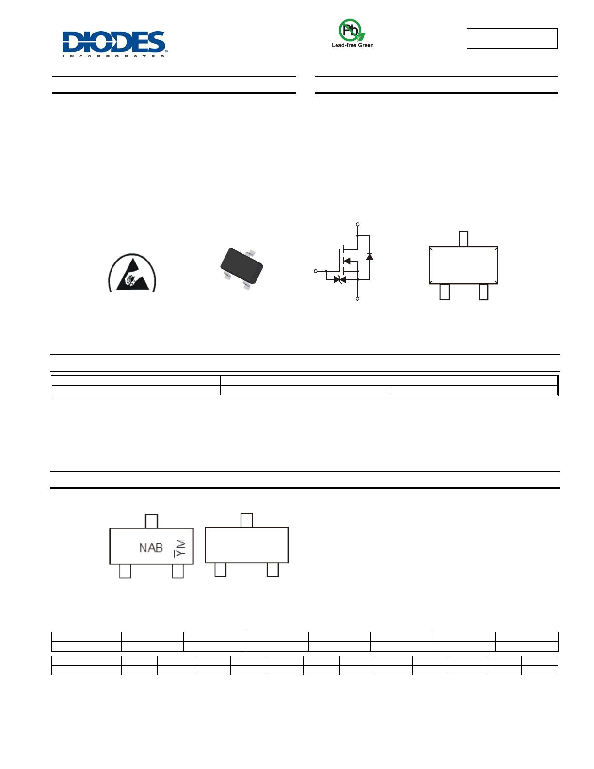
TOP VIEW
DMN2004W
N-CHANNEL ENHANCEMENT MODE MOSFET
Mechanical Data
Case: SOT-323
Case Material: Molded Plastic, “Green” Molding Compound.
UL Flammability Classification Rating 94V-0
Moisture Sensitivity: Level 1 per J-STD-020D
Terminals: Finish Matte Tin annealed over Alloy 42 leadframe.
Solderable per MIL-STD-202, Method 208
Terminal Connections: See Diagram
Weight: 0.006 grams (approximate)
SOT-323
Gate
Gate
Protection
Diode
EQUIVALENT CIRCUIT
Drain
Source
D
GS
TOP VIEW
Ordering Information (Note 4)
Part Number Case Packaging
DMN2004WK-7 SOT-323 3000/Tape & Reel
Notes: 1. No purposely added lead. Fully EU Directive 2002/95/EC (RoHS) & 2011/65/EU (RoHS 2) compliant.
2. See http://www.diodes.com/quality/lead_free.html for more information about Diodes Incorporated’s definitions of Halogen- and Antimony-free, "Green"
and Lead-free.
3. Halogen- and Antimony-free "Green” products are defined as those which contain <900ppm bromine, <900ppm chlorine (<1500ppm total Br + Cl) and
<1000ppm antimony compounds.
4. For packaging details, go to our website at http://www.diodes.com/products/packages.html
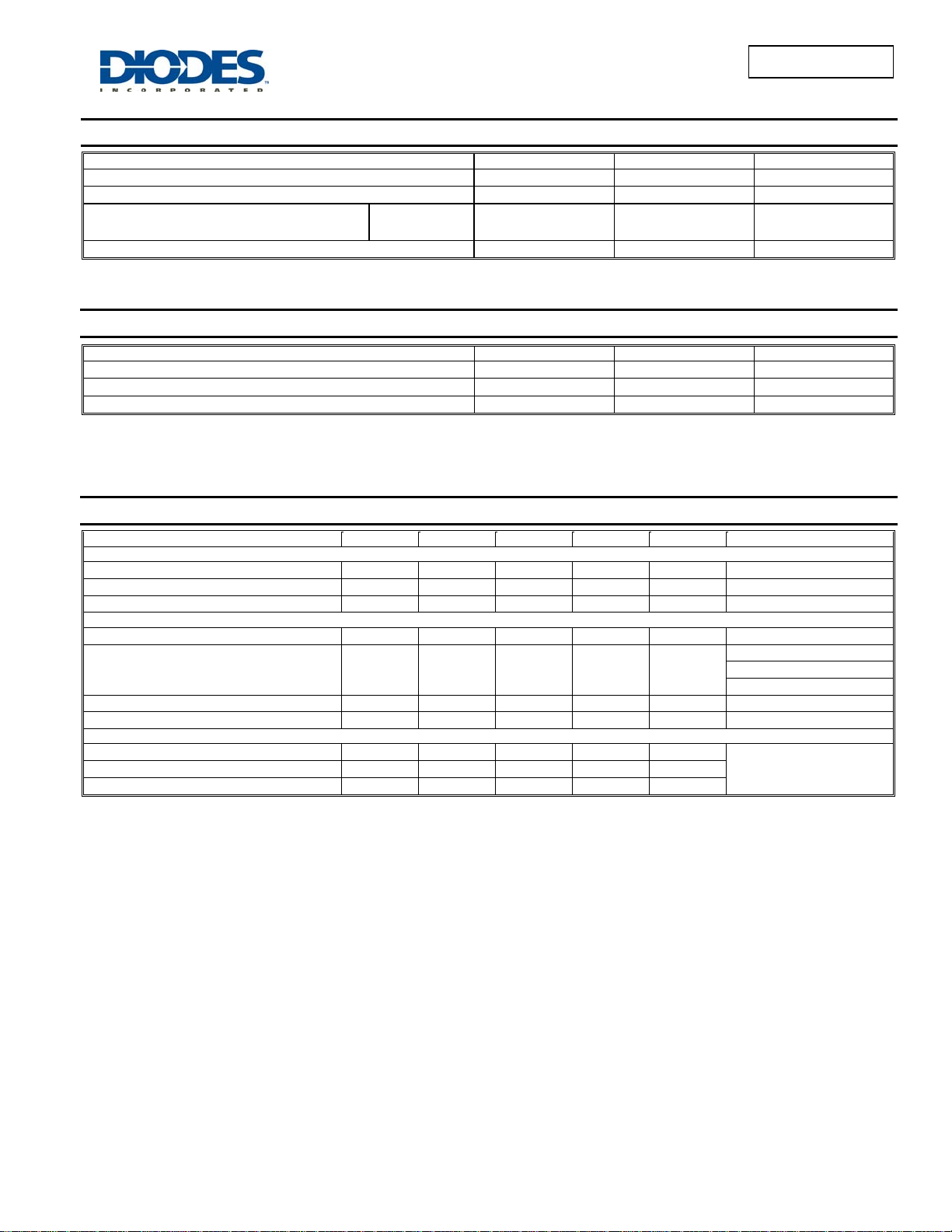
Marking Information
Date Code Key
Year 2009 2010 2011 2012 2013 2014 2015
Code W X Y Z A B C
Month Jan Feb Mar Apr May Jun Jul Aug Sep Oct Nov Dec
Code 1 2 3 4 5 6 7 8 9 O N D
Chengdu A/T Site
NAB
Shanghai A/T Site
NAB = Product Type Marking Code
YM = Date Code Marking for SAT (Shanghai Assembly/ Test site)
Y M = Date Code Marking for CAT (Chengdu Assembly/ Test site)
YM
Y or Y = Year (ex: A = 2013)
M = Month (ex: 9 = September)
DMN2004WK
Document number: DS30934 Rev. 5 - 2
1 of 6
www.diodes.com
September 2013
© Diodes Incorporated
K
)
DMN2004W
Maximum Ratings (@T
Drain-Source Voltage
Gate-Source Voltage
Drain Current (Note 5) Steady
State
Pulsed Drain Current (Note 6)
Thermal Characteristics (@T
Total Power Dissipation (Note 5)
Thermal Resistance, Junction to Ambient
Operating and Storage Temperature Range
Notes: 5. Device mounted on FR-4 PCB.
6. Pulse width 10S, Duty Cycle 1%.
Electrical Characteristics (@T
OFF CHARACTERISTICS (Note 7)
Drain-Source Breakdown Voltage
Zero Gate Voltage Drain Current
Gate-Source Leakage
ON CHARACTERISTICS (Note 7)
Gate Threshold Voltage
Static Drain-Source On-Resistance
Forward Transfer Admittance
Diode Forward Voltage (Note 7)
DYNAMIC CHARACTERISTICS(Note 8)
Input Capacitance
Output Capacitance
Reverse Transfer Capacitance
Notes: 7. Short duration pulse test used to minimize self-heating effect.
DMN2004WK
Document number: DS30934 Rev. 5 - 2
Characteristic Symbol Min Typ Max Unit Test Condition
8. Guaranteed by design. Not subject to production testing.
= +25°C, unless otherwise specified.)
A
Characteristic Symbol Value Units
20 V
±8 V
540
390
mA
1.5 A
TA = +25°C
TA = +85°C
= +25°C, unless otherwise specified.)
A
V
DSS
V
GSS
ID
I
DM
Characteristic Symbol Value Units
200 mW
625 °C/W
-55 to +150 °C
V
VGS = 0V, ID = 10A
VDS = 16V, VGS = 0V
μA
VGS = 4.5V, VDS = 0V
VDS = VGS, ID = 250A
VGS = 4.5V, ID = 540mA
Ω
VGS = 2.5V, ID = 500mA
VGS = 1.8V, ID = 350mA
ms
V
=10V, ID = 0.2A
DS
V
= 0V, IS = 115mA
GS
VDS = 16V, V
GS
= 0V
f = 1.0MHz
R
T
J, TSTG
= +25°C, unless otherwise specified.)
A
BV
V
DSS
I
DSS
I
GSS
GS(th
20
0.5
0.4
R
DS (ON)
|Yfs|
V
SD
C
iss
C
oss
C
rss
200
0.5
0.5
0.7
PD
JA
1 μA
1
1.0 V
0.55
0.70
0.9
1.4 V
150 pF
25 pF
20 pF
2 of 6
www.diodes.com
September 2013
© Diodes Incorporated
 Loading...