Diodes DMMT3904W User Manual

40V MATCHED PAIR NPN SMALL SIGNAL TRANSISTOR IN SOT363
Features
• BVceo > 40V
• I
= 200mA high Collector Current
C
• Pair of NPN transistors that are intrinsically matched (Note 1)
• 2% Matching on Current Gain (h
• 2mV Matching on Base-Emitter Voltage (V
• Fully internally isolated in a small surface mount package
• Totally Lead-Free & Fully RoHS Compliant (Notes 2 & 3)
• Halogen and Antimony Free. "Green" Device (Note 4)
• Qualified to AEC-Q101 Standards for High Reliability
• PPAP Capable (Note 5)
)
FE
SOT363
Top View
BE
)
DMMT3904W
Mechanical Data
• Case: SOT363
• Case Material: Molded Plastic, “Green” Molding Compound.
UL Flammability Classification Rating 94V-0
• Moisture Sensitivity: Level 1 per J-STD-020
• Terminals: Finish ⎯ Matte Tin Finish. Solderable per
MIL-STD-202, Method 208
• Weight: 0.006 grams (approximate)
e3
Applications
• Current mirrors
• Differential and instrumentation amplifiers
• Comparators
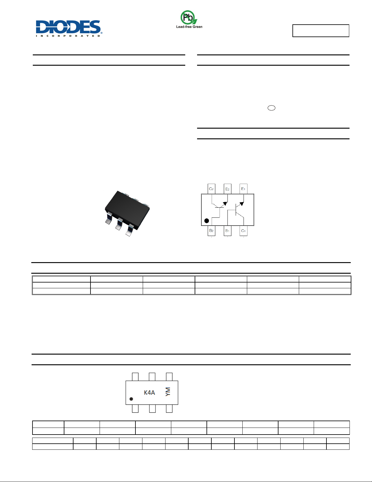
Device Schematic and Pin-Out
Top View
Ordering Information (Note 4 & 5)
Part Number Compliance Marking Reel Size (inches) Tape Width (mm) Quantity per Reel
DMMT3904W-7-F AEC-Q101 K4A 7 8 3,000
DMMT3904WQ-7-F Automotive K4A 7 8 3,000
Notes: 1. Intrinsically matched pair as this is built with adjacent die from the same wafer.
3. See http://www.diodes.com/quality/lead_free.html for more information about Diodes Incorporated’s definitions of Halogen- and Antimony-free, "Green"
and Lead-free.
4. Halogen- and Antimony-free "Green” products are defined as those which contain <900ppm bromine, <900ppm chlorine (<1500ppm total Br + Cl) and
<1000ppm antimony compounds.
5. Automotive products are AEC-Q101 qualified and are PPAP capable. Automotive, AEC-Q101 and standard products are electrically and thermally the
same, except where specified. For more information, please refer to http://www.diodes.com/quality/product_compliance_definitions/.
6. For packaging details, go to our website at http://www.diodes.com/products/packages.html.
2. No purposely added lead. Fully EU Directive 2002/95/EC (RoHS) & 2011/65/EU (RoHS 2) compliant.
Marking Information
Date Code Key
Year
Code X Y Z A B C D E
Month Jan Feb Mar Apr May Jun Jul Aug Sep Oct Nov Dec
Code 1 2 3 4 5 6 7 8 9 O N D
2010
2011 2012 2013 2014 2015
K4A = Product Type Marking Code
YM = Date Code Marking
Y = Year (ex: B = 2014)
M = Month (ex: 2 = February)
2016 2017
DMMT3904W
Document number: DS30311 Rev. 12 - 2
1 of 6
www.diodes.com
May 2014
© Diodes Incorporated

θ
Absolute Maximum Ratings (@T
Characteristic Symbol Value Unit
Collector-Base Voltage
Collector-Emitter Voltage
Emitter-Base Voltage
Collector Current
= +25°C unless otherwise specified.)
A
Thermal Characteristics – Total Device (@T
Characteristic Symbol Value Unit
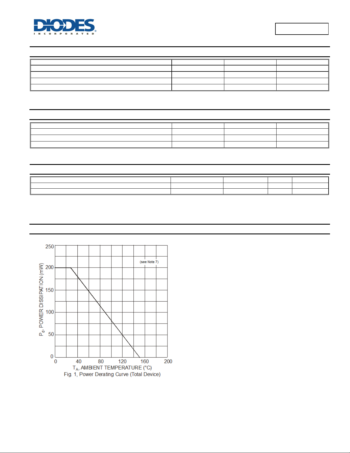
Power Dissipation (Note 7) Total Device
Thermal Resistance, Junction to Ambient (Note 7)
Operating and Storage Temperature Range
V
CBO
V
CEO
V
EBO
IC
= +25°C unless otherwise specified.)
A
PD
R
JA
TJ, T
STG
60 V
40 V
6.0 V
200 mA
200 mW
625 °C/W
-65 to +150 °C
DMMT3904W
ESD Ratings (Note 8)
Electrostatic Discharge - Human Body Model ESD HBM 4,000 V 3A
Electrostatic Discharge - Machine Model ESD MM 400 V C
Note: 7. For a device mounted on minimum recommended pad layout with 1oz copper that is on a single-sided 1.6mm FR4 PCB; the device is measured
under still air conditions whilst operating in a steady-state.
8. Refer to JEDEC specification JESD22-A114 and JESD22-A115.
Characteristic Symbol Value Unit JEDEC Class
Thermal Characteristics – Total Device
DMMT3904W
Document number: DS30311 Rev. 12 - 2
2 of 6
www.diodes.com
May 2014
© Diodes Incorporated
 Loading...