Diodes DMMT2907A User Manual

y
1
Features & Benefits
• BV
• I
• General purpose NPN transistors ideally suited for low power
• Dual transistors in a single SOT26 package taking half the
• Epitaxial planar die construction
• “Lead Free”, RoHS Compliant (Note 1)
• Halogen and Antimony Free. "Green" Device (Note 2)
• Qualified to AEC-Q101 Standards for High Reliability
> -60V
CEO
= -1A Peak Pulse Current
CM
amplification and switching applications
footprint of two equivalent transistors in SOT23
SOT26
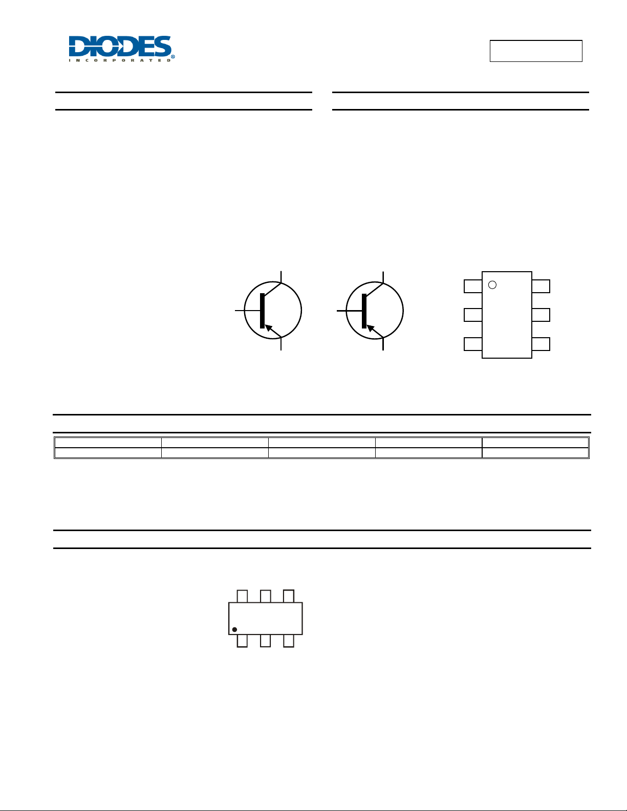
B1
ADVANCE INFORMATION
Top View
DMMT2907A
60V DUAL PNP SMALL SIGNAL SURFACE MOUNT TRANSISTOR
Mechanical Data
• Case: SOT26
• Case Material: Molded Plastic, “Green” Molding Compound.
UL Flammability Classification Rating 94V-0
• Moisture Sensitivity: Level 1 per J-STD-020
• Terminals: Solderable per MIL-STD-202, Method 208
• Lead Free Plating: Matte Tin Finish annealed over Copper
leadframe
• Weight: 0.015 grams (approximate)
B2
Device S
C2
B1
E2
B2
C1
E1
C2
E2
mbol
Top View
Pin-Out
C
E1
Ordering Information (Note 3)
Product Marking Reel size (inches) Tape width (mm) Quantity per reel
DMMT2907A-7 907 7 8 3,000
Notes: 1. No purposefully added lead.
2. Diodes Inc’s “Green” Policy can be found on our website at http://www.diodes.com
3. For packaging details, go to our website at http://www.diodes.com
Marking Information
907
907 = Product Type Marking Code
DMMT2907A
Document Number: DS35106 Rev: 1 - 2
1 of 7
www.diodes.com
April 2011
© Diodes Incorporated

θ
DMMT2907A
Maximum Ratings @T
= 25°C unless otherwise specified
A
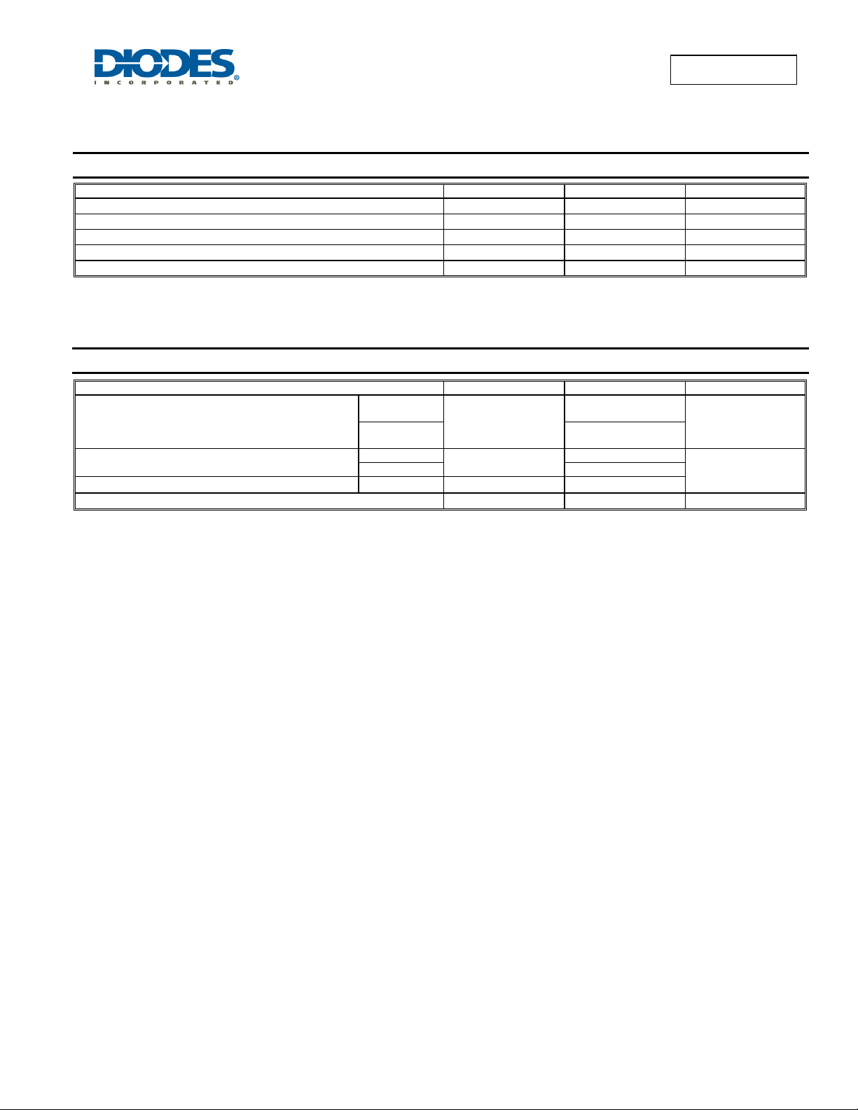
Characteristic Symbol Value Unit
Collector-Base Voltage
Collector-Emitter Voltage
Emitter-Base Voltage
Continuous Collector Current
Peak Pulsed Collector Current
V
CBO
V
CEO
V
EBO
I
C
I
CM
-60 V
-60 V
-5 V
-600 mA
-1 A
Thermal Characteristics @T
= 25°C unless otherwise specified
A
Characteristic Symbol Value Unit
Power Dissipation
Linear Derating Factor
Thermal Resistance, Junction to Ambient
ADVANCE INFORMATION
Thermal Resistance, Junction to Lead (Note 7)
Operating and Storage Temperature Range
Notes: 4. For a device surface mounted on 25mm x 25mm x 1.6mm FR4 PCB with high coverage of single sided 1oz copper, in still air conditions; the device is
measured when operating in a steady-state condition.
5. Same as note (4), except the device is measured at t ≤ 5 sec.
6. For a dual device with one active die.
7. Thermal resistance from junction to solder-point (at the end of the collector lead).
(Notes 5 & 6)
P
D
(Notes 4 & 6)
(Notes 5 & 6)
(Notes 4 & 6) 140
R
JA
θ
R
JL
T
, T
J
STG
1.28
10.3
0.90
7.14
97
113
-55 to +150
W
mW/°C
°C/W
°C
DMMT2907A
Document Number: DS35106 Rev: 1 - 2
2 of 7
www.diodes.com
April 2011
© Diodes Incorporated

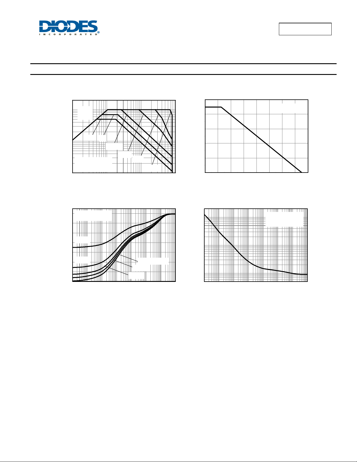
Thermal Characteristics
1
V
Limited
100m
25mm x 25m m 1oz Cu
T
Collector Current (A)
-I
amb
Single Pulse
C
10m
100m 1 10 100
-VCE Collector-Emitter Voltage (V)
ADVANCE INFORMATION
CE(sat)
DC
1s
100ms
10ms
=25°C
1ms
Safe Operating Area
100µs
1.0
25mm x 25mm
0.8
1oz Cu
0.6
0.4
0.2
0.0
0 20 40 60 80 100 120 140 160
Max Power Dissipation (W)
Temperature (°C)
Derating Curve
DMMT2907A
25mm x 25mm 1oz Cu
140
120
T
=25°C
amb
100
25mm x 25m m 1oz Cu
T
=25°C
amb
Single Pulse
100
D=0.5
80
10
60
D=0.2
40
20
0
100µ 1m 10m 100m 1 10 100 1k
Thermal Resistance (°C/W)
Pulse Width (s)
Transient Thermal Impedance
D=0.05
D=0.1
Single Pulse
1
Maximum Power (W)
100µ 1m 10m 100m 1 10 100 1k
Pulse Width (s)
Pulse Power Diss ipat ion
DMMT2907A
Document Number: DS35106 Rev: 1 - 2
3 of 7
www.diodes.com
April 2011
© Diodes Incorporated
 Loading...