

Page 1
485
C403
5LS
Y
NEW PRODUCT
Product Summary
Device
N-Channel 40V
P-Channel -40V
V
R
(BR)DSS
max
DS(ON)
45m @ V
58m @ VGS = 4.5V
65m @ V
100m @ VGS = -4.5V
= 10V
GS
= -10V
GS
Description
This new generation complementary MOSFET H-Bridge features low
on-resistance achievable with low gate drive.
Applications
• DC Motor Control
• DC-AC Inverters
NEW PRODUCT
ADVANCE INFORMATION
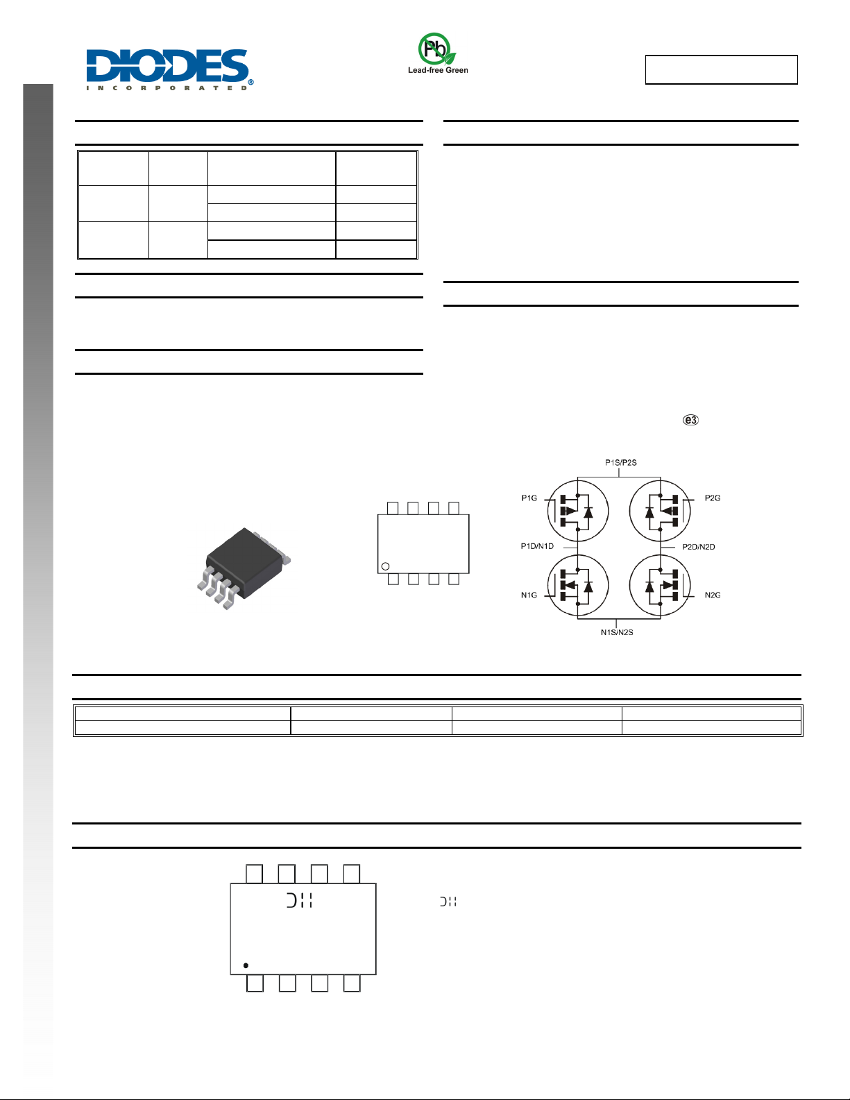
SO-8
Top View
Ordering Information (Note 4)
DMHC4035LSD
40V COMPLEMENTARY ENHANCEMENT MODE MOSFET H-BRIDGE
Features
I
max
D
TA = +25°C
4.5A
4A
-3.7A
-2.9A
• 2 x N + 2 x P channels in a SOIC package
• Low On-Resistance
• Low Input Capacitance
• Fast Switching Speed
• Totally Lead-Free & Fully RoHS compliant (Notes 1 & 2)
• Halogen and Antimony Free. “Green” Device (Note 3)
• Qualified to AEC-Q101 Standards for High Reliability
Mechanical Data
• Case: SO-8
• Case Material: Molded Plastic, "Green" Molding Compound.
UL Flammability Classification Rating 94V-0
• Moisture Sensitivity: Level 1 per J-STD-020
• Terminal Connections Indicator: See diagram
• Terminals: Finish ⎯ Matte Tin annealed over Copper leadframe.
• Weight: 0.074 grams (approximate)
N2D/P2D
P1S/P2S
P1G
P2G N2G
H-Bridge
N1S/N2S
N1D/P1D
N1G
Top View
Pin Configuration
Solderable per MIL-STD-202, Method 208
Internal Schematic
Part Number Compliance Case Packaging
DMHC4035LSD-13 Standard SO-8 2500/Tape & Reel
Notes: 1. No purposely added lead. Fully EU Directive 2002/95/EC (RoHS) & 2011/65/EU (RoHS 2) compliant.
2. See http://www.diodes.com/quality/lead_free.html for more information about Diodes Incorporated’s definitions of Halogen- and Antimony-free, "Green"
and Lead-free.
3. Halogen- and Antimony-free "Green” products are defined as those which contain <900ppm bromine, <900ppm chlorine (<1500ppm total Br + Cl) and
<1000ppm antimony compounds.
4. For packaging details, go to our website at http://www.diodes.com/products/packages.html.
Marking Information
DMHC4035LSD
Document number: DS36287 Rev. 1 - 2
1
Y WW
= Manufacturer’s Marking
C4035LS = Product Type Marking Code
www.diodes.com
YYWW = Date Code Marking
YY = Year (ex: 13 = 2013)
WW = Week (01 - 53)
1 of 9
January 2014
© Diodes Incorporated
Page 2
NEW PRODUCT
Thermal Characteristics (@T
A
Characteristic Symbol Value Units
Total Power Dissipation (Note 5)
Thermal Resistance, Junction to Ambient (Note 5)
Thermal Resistance, Junction to Case
Operating and Storage Temperature Range
Maximum Ratings N-CHANNEL (@T
Characteristic Symbol Value Units
Drain-Source Voltage
Gate-Source Voltage
Continuous Drain Current (Note 5) VGS = 10V
NEW PRODUCT
ADVANCE INFORMATION
Continuous Drain Current (Note 5) VGS = 4.5V
Maximum Continuous Body Diode Forward Current (Note 5)
Pulsed Drain Current (10µs pulse, duty cycle = 1%)
Maximum Ratings P-CHANNEL (@T
= +25°C, unless otherwise specified.)
Steady State
t<10s 53
= +25°C, unless otherwise specified.)
A
Steady
State
t<10s
Steady
State
t<10s
= +25°C, unless otherwise specified.)
A
T
= +25°C
A
T
= +70°C
A
T
= +25°C
A
T
= +70°C
A
T
= +25°C
A
T
= +70°C
A
T
= +25°C
A
T
= +70°C
A
T
V
DSS
V
GSS
I
I
I
I
I
I
DM
P
D
R
JA
θ
R
JC
θ
J, TSTG
D
D
D
D
S
DMHC4035LSD
1.5 W
85
°C/W
15
-55 to +150 °C
40 V
±20 V
4.5
3.5
5.8
4.5
4
3.1
5.1
4
1.5
25
A
A
A
A
A
A
Characteristic Symbol Value Units
Drain-Source Voltage
Gate-Source Voltage
Continuous Drain Current (Note 5) VGS = -10V
Continuous Drain Current (Note 5) VGS = -4.5V
Steady
State
t<10s
Steady
State
t<10s
T
= +25°C
A
T
= +70°C
A
T
= +25°C
A
T
= +70°C
A
T
= +25°C
A
= +70°C
T
A
T
= +25°C
A
T
= +70°C
A
Maximum Continuous Body Diode Forward Current (Note 5)
Pulsed Drain Current (10µs pulse, duty cycle = 1%)
Note: 5. Device mounted on FR-4 substrate PC board, 2oz copper, with 1inch square copper plate.
V
DSS
V
GSS
I
D
I
D
I
D
I
D
I
S
I
DM
-40 V
±20 V
-3.7
-2.9
-4.8
-3.8
-2.9
-2.3
-3.9
-3.0
-1.5
-15
A
A
A
A
A
A
DMHC4035LSD
Document number: DS36287 Rev. 1 - 2
2 of 9
www.diodes.com
January 2014
© Diodes Incorporated
Page 3
NEW PRODUCT
Electrical Characteristics N-CHANNEL (@T
Characteristic Symbol Min Typ Max Unit Test Condition
OFF CHARACTERISTICS (Note 6)
Drain-Source Breakdown Voltage
Zero Gate Voltage Drain Current
Gate-Source Leakage
ON CHARACTERISTICS (Note 6)
Gate Threshold Voltage
Static Drain-Source On-Resistance
Diode Forward Voltage
DYNAMIC CHARACTERISTICS (Note 7)
Input Capacitance
Output Capacitance
Reverse Transfer Capacitance
Gate resistance
Total Gate Charge (VGS = 4.5V) Qg
Total Gate Charge (VGS = 10V) Qg
Gate-Source Charge
NEW PRODUCT
Gate-Drain Charge
Turn-On Delay Time
ADVANCE INFORMATION
Turn-On Rise Time
Turn-Off Delay Time
Turn-Off Fall Time
Reverse Recovery Time
Reverse Recovery Charge
Electrical Characteristics P-CHANNEL (@T
Characteristic Symbol Min Typ Max Unit Test Condition
OFF CHARACTERISTICS (Note 6)
Drain-Source Breakdown Voltage
Zero Gate Voltage Drain Current
Gate-Source Leakage
ON CHARACTERISTICS (Note 6)
Gate Threshold Voltage
Static Drain-Source On-Resistance
Diode Forward Voltage
DYNAMIC CHARACTERISTICS (Note 7)
Input Capacitance
Output Capacitance
Reverse Transfer Capacitance
Gate resistance
Total Gate Charge (VGS = -4.5V) Qg
Total Gate Charge (VGS = -10V) Qg
Gate-Source Charge
Gate-Drain Charge
Turn-On Delay Time
Turn-On Rise Time
Turn-Off Delay Time
Turn-Off Fall Time
Reverse Recovery Time
Reverse Recovery Charge
Notes: 6. Short duration pulse test used to minimize self-heating effect.
7. Guaranteed by design. Not subject to product testing.
= +25°C, unless otherwise specified.)
A
BV
DSS
I
DSS
I
GSS
V
GS(th)
R
DS (ON)
V
SD
C
iss
C
oss
C
rss
R
g
Q
gs
Q
gd
t
D(on)
t
r
t
D(off)
t
f
t
rr
Q
rr
= +25°C, unless otherwise specified.)
A
BV
DSS
I
DSS
I
GSS
V
GS(th)
R
DS (ON)
V
SD
C
iss
C
oss
C
rss
R
g
Q
gs
Q
gd
t
D(on)
t
r
t
D(off)
t
f
t
rr
Q
rr
40
— —
— —
1 — 3 V
—
—
—
— 574
—
—
—
—
—
—
—
—
—
—
—
—
—
-40
— —
— —
-1 — -3 V
—
—
—
—
—
—
—
—
—
—
—
—
—
—
—
—
—
— —
26 45
35 58
0.7 1 V
87.8
38.7
1.6
5.9
12.5
1.7
2.2
3.1
2.6
15
5.5
6.5
1.2
—
49 65
73 100
-0.7 -1.2 V
587
88.1
40.2
12.3
5.4
11.1
1.5
2
3.6
2.9
36.3
15.3
15.5
16.9
V
1 A
±100 nA
m
—
—
pF
—
—
—
—
—
nC
—
—
—
—
ns
—
—
—
ns
nC
— V
-1 A
±100 nA
m
—
—
—
—
—
—
—
—
—
—
—
—
—
—
pF
pF
pF
nC
nC
nC
nC
ns
ns
ns
ns
ns
nC
DMHC4035LSD
VGS = 0V, ID = 250A
VDS = 40V, VGS = 0V
VGS = ±20V, VDS = 0V
VDS = VGS, ID = 250A
V
= 10V, ID = 3.9A
GS
V
= 4.5V, ID = 3.5A
GS
VGS = 0V, IS = 1.25A
V
= 20V, VGS = 0V,
DS
f = 1MHz
VDS = 0V, VGS = 0V, f = 1MHz
= 20V, ID = 3.9A
V
DS
V
= 20V, VGS = 10V,
DD
= 20, RG = 6,
R
L
I
= 3.9A, di/dt = 500A/s
F
VGS = 0V, ID = -250A
VDS = -40V, VGS = 0V
V
= ±20V, VDS = 0V
GS
VDS = VGS, ID = -250A
V
= -10V, ID = -4.2A
GS
= -4.5V, ID = -3.3A
V
GS
V
= 0V, IS = -1A
GS
V
= -20V, VGS = 0V,
DS
f = 1MHz
VDS = 0V, VGS = 0V, f = 1MHz
V
= -20V, ID = -4.2A
DS
V
= -15V, VGS = -10V,
DD
= 6, ID = -1A
R
G
I
= -4.2A, di/dt = 500A/s
F
DMHC4035LSD
Document number: DS36287 Rev. 1 - 2
3 of 9
www.diodes.com
January 2014
© Diodes Incorporated
Page 4
RAIN
C
URREN
T
R
C
URRENT
R
R
OUR
ON-R
R
RAIN-SOUR
CE O
N-R
TAN
C
R
R
OUR
ON-R
R
R
O
U
R
C
DMHC4035LSD
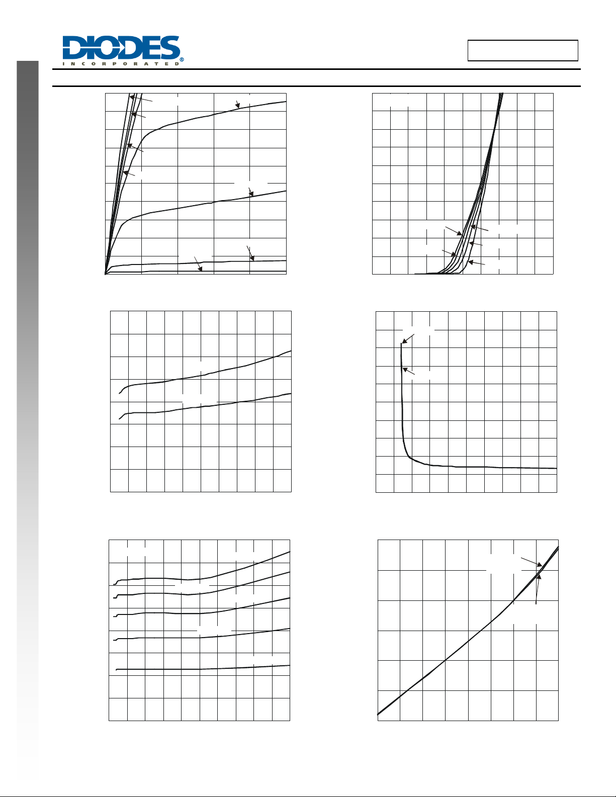
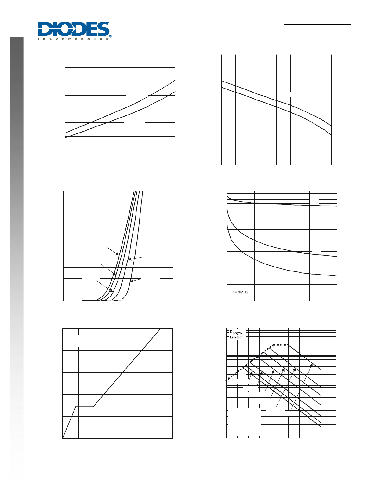
Typical Characteristics - N-CHANNEL
20
18
V= 10V
GS
V= 5.0V
GS
V= 3.5V
GS
16
14
(A)
12
10
V= 4.5V
GS
V= 4.0V
GS
V= 3.0V
GS
8
6
D
I, D
4
V= 2.3V
2
GS
V= 2.5V
GS
NEW PRODUCT
0
012345
V , DRAIN-SOURCE VOLTAGE (V)
DS
NEW PRODUCT
Figure 1 Typical Output Characteristics
0.05
Ω
0.045
ADVANCE INFORMATION
0.04
ESISTANCE ( )
0.035
0.03
CE
0.025
AIN-S
0.02
, D
0.015
DS(ON)
0.01
0 2 4 6 8 10 12 14 16 18 20
I , DRAIN-SOURCE CURRENT (A)D
Figure 3 Typical On-Resistance vs.
Drain Current and Gate Voltage
0.08
Ω
V = 4.5VGS
0.07
0.06
ESISTANCE ( )
0.05
0.04
CE
0.03
AIN-S
0.02
, D
0.01
DS(ON)
0
0 2 4 6 8 10121416 1820
Figure 5 Typical On-Resistance vs.
Drain Current and Temperature
DMHC4035LSD
Document number: DS36287 Rev. 1 - 2
V = 4.5VGS
V = 10VGS
T = 150°C
A
T = 125°C
A
T = 25°C
I , DRAIN CURRENT (A)
D
T = 85°C
A
A
T = -55°C
A
4 of 9
www.diodes.com
20
V= 5.0V
DS
18
16
14
(A)
12
10
8
AIN
6
D
I, D
4
2
0
0 0.5 1 1.5 2 2.5 3 3.5 4 4.5 5
T = 150°C
A
T = 125°C
A
V , GATE-SOURCE VOLTAGE (V)
GS
T = 85°C
A
T = 25°C
A
T = -55°C
A
Figure 2 Typical Transfer Characteristics
0.2
Ω
0.18
E ( )
I = 3.9AD
0.16
0.14
ESIS
I = 3.5AD
0.12
0.1
0.08
0.06
0.04
, D
0.02
DS(ON)
0
02468101214161820
V , GATE-SOURCE VOLTAGE (V)GS
Figure 4 Typical Transfer Characteristics
1.8
V=V
10
GS
I= 10A
1.6
D
E
1.4
AIN-S
1.2
, D
1
DS(ON)
ON-RESISTANCE (NORMALIZED)
0.8
0.6
-50 -25 0 25 50 75 100 125 150
T , JUNCTION TEMPERATURE ( C)
J
Figure 6 On- Resistance Variation with Temperature
V=5V
GS
I= 5A
D
°
January 2014
© Diodes Incorporated
Page 5
R
R
OUR
CE ON-R
TANC
GATE THRESH
O
OLT
G
OUR
CE CUR
RENT
C
UNC
TION CAPACITANC
G
TE T
H
R
H
O
O
TAG
R
C
U
R
RENT
NEW PRODUCT
NEW PRODUCT
ADVANCE INFORMATION
DMHC4035LSD
0.08
Ω
E ( )
0.07
2.5
E (V)
A
0.06
V=5V
ESIS
0.05
GS
I= 5A
D
0.04
V=V
10
0.03
AIN-S
0.02
GS
I= 10A
D
2
I= 1mA
LD V
1.5
I = 250µA
D
D
1
, D
0.01
DS(ON)
0
-50 -25 0 25 50 75 100 125 150
T , JUNCTION TEMPERATURE ( C)
J
Figure 7 On-Resistance Variation with Temperature
20
18
°
GS(th)
V,
0.5
-50 -25 0 25 50 75 100 125 150
T , JUNCTION TEMPERATURE ( C)
J
°
Figure 8 Gate Threshold Variation vs. Ambient Temperature
1000
C
iss
16
(A)
14
E (pF)
12
T = 150°C
A
T = 125°C
A
T= 85°C
A
T= 25°C
A
T = -55°C
A
S
I, S
10
8
6
4
2
0
0 0.3 0.6 0.9 1.2 1.5
V , SOURCE-DRAIN VOLTAGE (V)
SD
Figure 9 Diode Forward Voltage vs. Current
10
V = 20V
DS
I= A
3.9
E (V)
D
8
L
6
LD V
ES
4
A
2
GS
V
0
02468101214
Q(nC)
, TOTAL GATE CHARGE
g
Figure 11 Gate Charge
100
, J
T
10
0 5 10 15 20 25 30 35 40
V , DRAIN-SOURCE VOLTAGE (V)
DS
Figure 10 Typical Junction Capacitance
C
oss
C
rss
100
10
(A)
DC
P = 10s
W
1
AIN
D
0.1
I, D
0.01
0.1 1 10 100
P = 1s
W
P = 100ms
W
P = 10ms
W
P = 1ms
T = 150°C
J(max)
T = 25°C
A
V = 4.5V
GS
Single Pulse
DUT on 1 * MRP Board
V , DRAIN-SOURCE VOLTAGE (V)
DS
W
P = 100µs
W
Figure 12 SOA, Safe Operation Area
DMHC4035LSD
Document number: DS36287 Rev. 1 - 2
5 of 9
www.diodes.com
January 2014
© Diodes Incorporated
Page 6

R
CUR
RENT
R
CUR
RENT
R
R
OUR
ON-R
R
R
OUR
CE ON-R
TANC
R
R
OUR
ON-R
R
RAIN
OUR
C
NEW PRODUCT
NEW PRODUCT
ADVANCE INFORMATION
DMHC4035LSD
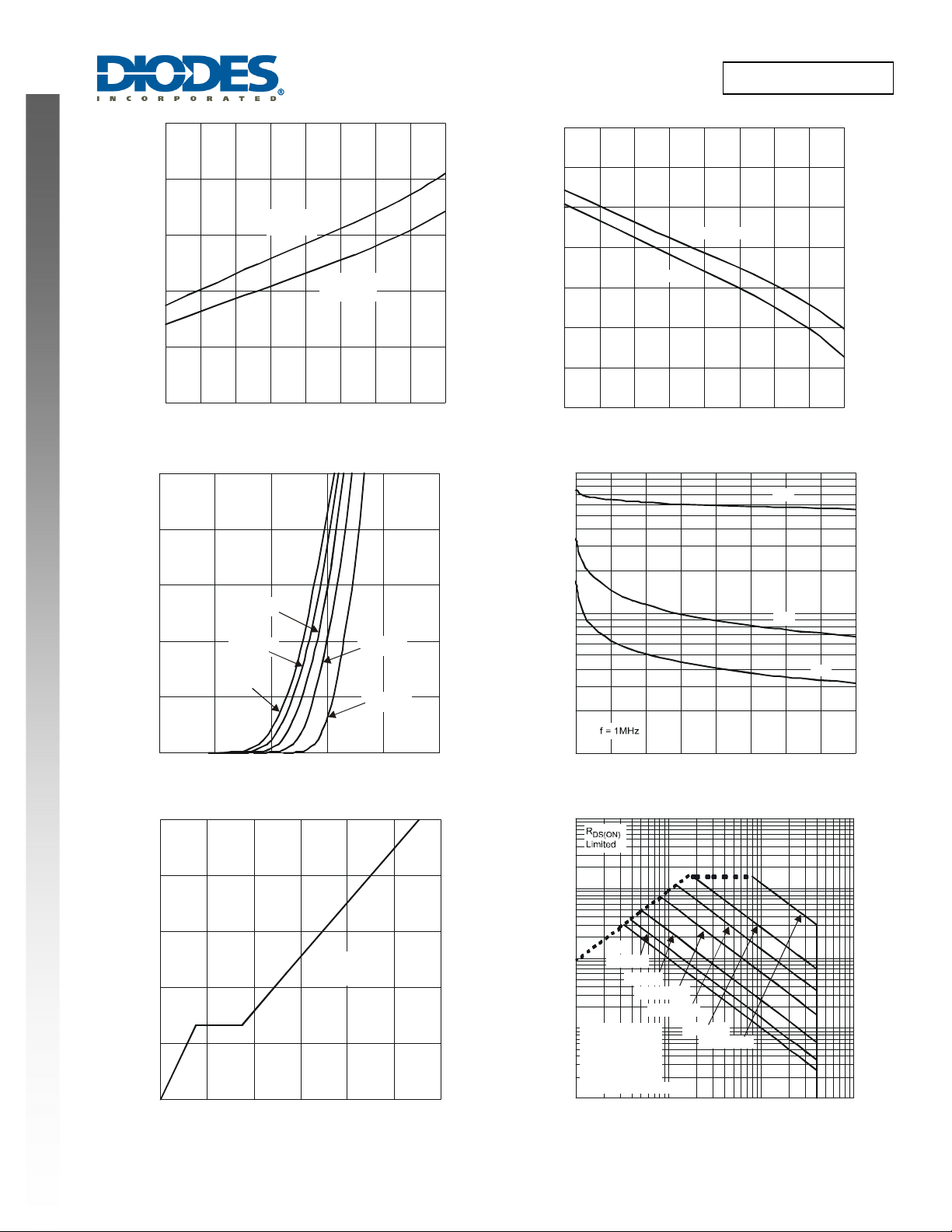
Typical Characteristics - P-CHANNEL
15
12
V= -10V
GS
V = -5.0V
GS
V= -3.5V
GS
(A)
9
V= -3.0V
GS
6
AIN
D
-I , D
V = -2.5V
GS
3
V = -2.0V
GS
0
012345
-V , DRAIN -SOURCE VOLTAGE (V)
DS
Figure 13 Typical Output Characteristics
0.2
Ω
0.18
0.16
15
V = -5.0V
DS
12
(A)
9
6
AIN
D
-I , D
3
0
0123 45
T = 150°C
A
T = 125°C
A
-V , GATE-SOURCE VOLTAGE (V)
GS
T = 85°C
A
T = 25°C
A
T = -55°C
A
Figure 14 Typical Transfer Characteristics
0.5
Ω
0.45
E ( )
I = -4.2A
D
0.4
0.14
ESISTANCE ( )
0.12
V = -4.5V
CE
0.1
GS
0.08
0.06
AIN-S
0.04
, D
0.02
DS(ON)
0
0 2 4 6 8 101214 1618 20
-I , DRAIN SOURCE CURRENT (A)
D
V = -10V
GS
Figure 15 Typical On-Resistance vs.
Drain Current and Gate Voltage
0.2
Ω
V = -4.5V
GS
0.18
ESISTANCE ( )
CE
0.16
0.14
0.12
0.1
T = 125CA°
T = 150CA°
T = 85CA°
T = 25CA°
0.08
0.06
AIN-S
0.04
, D
0.02
DS(ON)
0
0 3 6 9 12 15
-I , DRAIN SOURCE CURRENT (A)
D
T = -55CA°
Figure 17 Typical On-Resistance vs.
Drain Current and Temperature
DMHC4035LSD
Document number: DS36287 Rev. 1 - 2
6 of 9
www.diodes.com
0.35
ESIS
0.3
0.25
I = -3.3A
D
0.2
0.15
AIN-S
0.1
, D
0.05
DS(ON)
0
0 2 4 6 8 101214161820
-V , GATE-SOURCE VOLTAGE (V)
GS
Figure 16 Typical Transfer Characteristics
1.8
V = -10V
GS
I = -10A
1.6
D
E
1.4
-S
1.2
, D
1
DS(ON)
ON-RESISTANCE (NORMALIZED)
0.8
0.6
-50 -25 0 25 50 75 100 125 150
T , JUNCTION TEMPERATURE ( C)
J
Figure 18 On-Resistance Variation with Temperature
V = -5V
GS
I = -5A
D
°
January 2014
© Diodes Incorporated
Page 7
R
RAIN-SOUR
CE O
N-R
TAN
C
GATE THRESH
O
OLTAG
OUR
CE CUR
REN
T
C
UNC
TION CAPACITANC
F
G
T
OUR
C
OLT
G
R
C
U
R
RENT
NEW PRODUCT
NEW PRODUCT
ADVANCE INFORMATION
DMHC4035LSD
0.15
2
Ω
E ( )
ESIS
0.12
0.09
0.06
-
V=5V
GS
-5
I= A
D
V= -10V
GS
I= A
-10
D
1.8
E (V)
1.6
-I = 250µA
1.4
LD V
D
-I = 1m AD
1.2
1
0.03
, D
DS(on)
0
-50 -25 0 25 50 75 100 125 150
T , JUNCTION TEMPERATURE ( C)
J
Figure 19 On-Resistance Variation with Temperature
15
°
0.8
GS(TH)
V,
0.6
-50 -25 0 25 50 75 100 125 150
T , AMBIENT TEMPERATURE (°C)
A
Figure 20 Gate Threshold Variation vs. Ambient Temperature
1000
C
iss
)
12
(A)
E (p
9
T= 85CA°
6
S
-I , S
3
0
0 0.3 0.6 0.9 1.2 1.5
T= 125CA°
T= 150CA°
-V , SOURCE-DRAIN VOLTAGE (V)
SD
T= 25CA°
T= -55CA°
Figure 21 Diode Forward Voltage vs. Current
10
8
E (V)
A
6
E V
V = -20V
DS
I = -4.2A
4
E-S
D
A
GS
2
-V ,
0
024681012
Q , TOTAL GATE CHARGE (nC)
g
Figure 23 Gate-Charge Characteristics
100
, J
T
10
0 5 10 15 20 25 30 35 40
-V , DRAIN-SOURCE VOLTAGE (V)
DS
C
oss
Figure 22 Typical Junction Capacitance
100
10
(A)
DC
P = 10s
W
P = 1s
W
P = 100ms
W
P = 10ms
W
T = 150°C
J(max)
T = 25°C
A
V = -4.5V
GS
Single Pulse
DUT on 1 * MRP Board
P = 1ms
W
P = 100µs
W
0.1 1 10 100
-V , DRAIN-SOURCE VOLTAGE (V)
DS
AIN
D
-I , D
1
0.1
0.01
Figure 24 SOA, Safe Operation Area
C
rss
DMHC4035LSD
Document number: DS36287 Rev. 1 - 2
7 of 9
www.diodes.com
January 2014
© Diodes Incorporated
Page 8

T
R
T T
HER
R
TANC
NEW PRODUCT
NEW PRODUCT
Package Outline Dimensions
Please see AP02002 at http://www.diodes.com/datasheets/ap02002.pdf for latest version.
ADVANCE INFORMATION
1
D = 0.9
D = 0.7
E
D = 0.5
D = 0.3
ESIS
0.1
D = 0.1
MAL
D = 0.05
D = 0.02
0.01
D = 0.01
D = 0.005
ANSIEN
D = Single Pulse
r(t),
0.001
0.00001 0.0001 0.001 0.01 0.1 1 10 100 1000
t1, PULSE DURATION TIME (sec)
Figure 25 Transient Thermal Resistance
E1
E
A1
Detail ‘A’
L
0.254
Gauge Plan e
Seating Plane
7°~9
A2
e
b
D
A
A3
h
°
45
°
Detail ‘A’
Suggested Pad Layout
Please see AP02001 at http://www.diodes.com/datasheets/ap02001.pdf for the latest version.
X
C1
C2
Y
R (t) = r(t) * R
θθ
JA JA
R = 110°C/W
θ
JA
Duty Cycle, D = t1/ t2
Dim Min Max
Dimensions Value (in mm)
X 0.60
Y 1.55
C1 5.4
C2 1.27
SO-8
A - 1.75
A1 0.10 0.20
A2 1.30 1.50
A3 0.15 0.25
b 0.3 0.5
D 4.85 4.95
E 5.90 6.10
E1 3.85 3.95
e 1.27 Typ
h - 0.35
L 0.62 0.82
0° 8°
θ
All Dimensions in mm
DMHC4035LSD
DMHC4035LSD
Document number: DS36287 Rev. 1 - 2
8 of 9
www.diodes.com
January 2014
© Diodes Incorporated
Page 9

NEW PRODUCT
DIODES INCORPORATED MAKES NO WARRANTY OF ANY KIND, EXPRESS OR IMPLIED, WITH REGARDS TO THIS DOCUMENT,
INCLUDING, BUT NOT LIMITED TO, THE IMPLIED WARRANTIES OF MERCHANTABILITY AND FITNESS FOR A PARTICULAR PURPOSE
(AND THEIR EQUIVALENTS UNDER THE LAWS OF ANY JURISDICTION).
Diodes Incorporated and its subsidiaries reserve the right to make modifications, enhancements, improvements, corrections or other changes
without further notice to this document and any product described herein. Diodes Incorporated does not assume any liability arising out of the
application or use of this document or any product described herein; neither does Diodes Incorporated convey any license under its patent or
trademark rights, nor the rights of others. Any Customer or user of this document or products described herein in such applications shall assume
all risks of such use and will agree to hold Diodes Incorporated and all the companies whose products are represented on Diodes Incorporated
website, harmless against all damages.
Diodes Incorporated does not warrant or accept any liability whatsoever in respect of any products purchased through unauthorized sales channel.
Should Customers purchase or use Diodes Incorporated products for any unintended or unauthorized application, Customers shall indemnify and
hold Diodes Incorporated and its representatives harmless against all claims, damages, expenses, and attorney fees arising out of, directly or
indirectly, any claim of personal injury or death associated with such unintended or unauthorized application.
Products described herein may be covered by one or more United States, international or foreign patents pending. Product names and markings
noted herein may also be covered by one or more United States, international or foreign trademarks.
This document is written in English but may be translated into multiple languages for reference. Only the English version of this document is the
final and determinative format released by Diodes Incorporated.
NEW PRODUCT
ADVANCE INFORMATION
Diodes Incorporated products are specifically not authorized for use as critical components in life support devices or systems without the express
written approval of the Chief Executive Officer of Diodes Incorporated. As used herein:
A. Life support devices or systems are devices or systems which:
1. are intended to implant into the body, or
labeling can be reasonably expected to result in significant injury to the user.
B. A critical component is any component in a life support device or system whose failure to perform can be reasonably expected to cause the
failure of the life support device or to affect its safety or effectiveness.
Customers represent that they have all necessary expertise in the safety and regulatory ramifications of their life support devices or systems, and
acknowledge and agree that they are solely responsible for all legal, regulatory and safety-related requirements concerning their products and any
use of Diodes Incorporated products in such safety-critical, life support devices or systems, notwithstanding any devices- or systems-related
information or support that may be provided by Diodes Incorporated. Further, Customers must fully indemnify Diodes Incorporated and its
representatives against any damages arising out of the use of Diodes Incorporated products in such safety-critical, life support devices or systems.
Copyright © 2014, Diodes Incorporated
www.diodes.com
2. support or sustain life and whose failure to perform when properly used in accordance with instructions for use provided in the
IMPORTANT NOTICE
LIFE SUPPORT
DMHC4035LSD
DMHC4035LSD
Document number: DS36287 Rev. 1 - 2
9 of 9
www.diodes.com
January 2014
© Diodes Incorporated
 Loading...