Diodes DMG9926UDM User Manual

θ
Please click here to visit our online spice models database.
Features
• Low Gate Charge
• Low R
• 28mΩ @V
• 32mΩ @V
• 40mΩ @V
• Low Input/Output Leakage
• Lead Free By Design/RoHS Compliant (Note 3)
• Qualified to AEC-Q101 Standards for High Reliability
• "Green" Device (Note 4)
NEW PRODUCT
DS(ON)
:
= 4.5V
GS
= 2.5V
GS
= 1.8V
GS
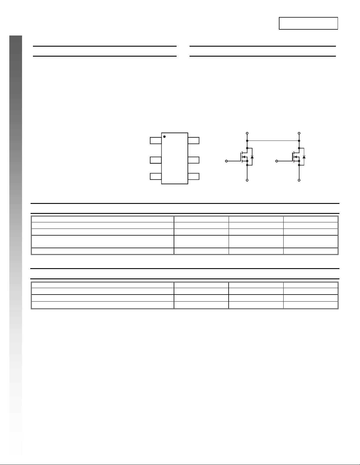
TOP VIEW
SOT-26
S
1
D/1D
2
S
2
TOP VIEW
Pin Configuration
DMG9926UDM
DUAL N-CHANNEL ENHANCEMENT MODE MOSFET
Mechanical Data
• Case: SOT-26
• Case Material - Molded Plastic, “Green” Molding
Compound. UL Flammability Classification Rating 94V-0
• Moisture Sensitivity: Level 1 per J-STD-020D
• Terminals: Finish – Matte Tin annealed over Copper
leadframe. Solderable per MIL-STD-202, Method 208
• Terminal Connections: See Diagram
• Marking Information: See Page 4
• Ordering Information: See Page 4
• Weight: 0.008 grams (approximate)
D1 D2
G
1
D/1D
2
G
2
G1
G2
S1 S2
Equivalent Circuit
Maximum Ratings @T
= 25°C unless otherwise specified
A
Characteristic Symbol Value Unit
Drain-Source Voltage
Gate-Source Voltage
Drain Current (Note 1) Continuous TA = 25°C
T
Pulsed Drain Current (Note 2)
Thermal Characteristics @T
= 25°C unless otherwise specified
A
Characteristic Symbol Value Unit
Total Power Dissipation (Note 1)
Thermal Resistance, Junction to Ambient (Note 1) t ≤10s
Operating and Storage Temperature Range
Notes: 1. Device mounted on 1"x1", FR-4 PC board with 2 oz. Copper and test pulse width t ≤10s.
2. Repetitive Rating, pulse width limited by junction temperature.
3. No purposefully added lead.
4. Diodes Inc's "Green" policy can be found on our website at http://www.diodes.com/products/lead_free/index.php.
DMG9926UDM
Document number: DS31770 Rev. 4 - 2
= 70°C
A
www.diodes.com
1 of 6
V
DSS
V
GSS
I
D
I
DM
P
D
R
JA
, T
T
J
STG
20 V
±8
4.2
3.2
V
A
30 A
0.98 W
128
-55 to +150
°C /W
°C
June 2009
© Diodes Incorporated

)
g
g
g
)
r
)
R
C
U
R
RENT
RAIN CUR
R
N
T
Electrical Characteristics @T
STATIC CHARACTERISTICS
Drain-Source Breakdown Voltage
Zero Gate Voltage Drain Current
Gate-Body Leakage Current
Gate Threshold Voltage
Static Drain-Source On-Resistance (Note 5)
Forward Transfer Admittance
Diode Forward Voltage (Note 5)
DYNAMIC CHARACTERISTICS (Note 6)
Input Capacitance
Output Capacitance
Reverse Transfer Capacitance
Gate Resisitance
NEW PRODUCT
SWITCHING CHARACTERISTICS
Total Gate Charge
Gate-Source Charge
Gate-Drain Charge
Turn-On Delay Time
Turn-On Rise Time
Turn-Off Delay Time
Turn-Off Fall Time
Notes: 5. Test pulse width t = 300ms.
6. Guaranteed by design. Not subject to production testing.
30
Characteristic Symbol Min Typ Max Unit Test Condition
= 25°C unless otherwise specified
A
20
BV
DSS
I
DSS
I
GSS
V
GS(th
R
DS (ON)
|Y
FS
V
SD
C
iss
C
oss
C
rss
R
G
Q
Q
s
Q
d
t
D(on
t
⎯
t
D(off
t
⎯
f
⎯ ⎯
⎯ ⎯
0.5
⎯
| ⎯
⎯
⎯
⎯
⎯
⎯
⎯
⎯
⎯
⎯
⎯
⎯ ⎯
1
±100
⎯
22
25
31
7
0.9 V
28
32
40
⎯
V
μA
nA
mΩ
S
0.7 0.9 V
856
83
78
1.32
8.3
1.3
3.1
8.4
8.2
40.4
8.9
⎯
⎯
⎯
⎯ Ω
⎯
⎯
⎯
⎯
⎯
⎯
⎯
pF
pF
pF
nC
nC
nC
ns
ns
ns
ns
20
DMG9926UDM
ID = 250μA, VGS = 0V
V
= 20V, VGS = 0V
DS
V
= 0V, VGS = ±8V
DS
V
= VGS, ID = 250μA
DS
= 4.5V, ID = 8.2A
V
GS
= 2.5V, ID = 3.3A
V
GS
V
= 1.8V, ID = 2.0A
GS
V
= 10V, ID = 4A
DS
IS = 2.25A, V
= 10V, VGS = 0V
V
DS
f = 1.0MHz
VGS = 0V, V
= 4.5V, V
V
GS
= 10V, V
V
DD
R
= 10Ω, RG = 6Ω
L
= 0V
GS
= 0V, f = 1MHz
DS
= 10V, ID = 8.2A
DS
= 4.5V,
GS
25
(A)
20
V = 8.0V
GS
V = 4.5V
GS
V = 3.0V
V = 2.5V
GS
V = 2.0V
GS
16
GS
V = 5V
DS
(A)
12
E
15
AIN
10
D
I, D
V = 1.5V
GS
5
0
0 0.4 0.8 1.2 1.6 2
V , DRAIN-SOURCE VOLTAGE (V)
DS
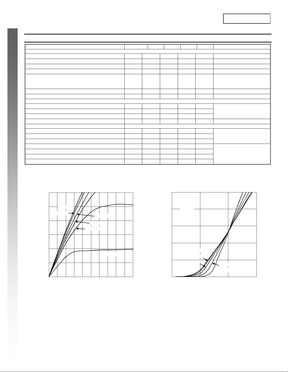
Fig. 1 Typical Output Ch ar acterist ic s
8
T = 150°C
D
I, D
4
A
T = 125°C
A
T = 85°C
A
T = 25°C
A
T = -55°C
A
0
0.5 1 1.5 2
V , GATE SOURCE VOLT AGE (V)
GS
Fig. 2 Typical Transfer Characteristics
DMG9926UDM
Document number: DS31770 Rev. 4 - 2
2 of 6
www.diodes.com
June 2009
© Diodes Incorporated
 Loading...