Diodes DMG4N65CT User Manual

Product Summary
Package
TO220-3 4.0 A
V
(BR)DSS
650V
R
3.0Ω@V
DS(ON)
GS
= 10V
Description
This new generation complementary MOSFET features low onresistance and fast switching, making it ideal for high efficiency power
management applications.
Applications
• Motor control
• Backlighting
• DC-DC Converters
• Power management functions
ADVANCE INFORMATIO
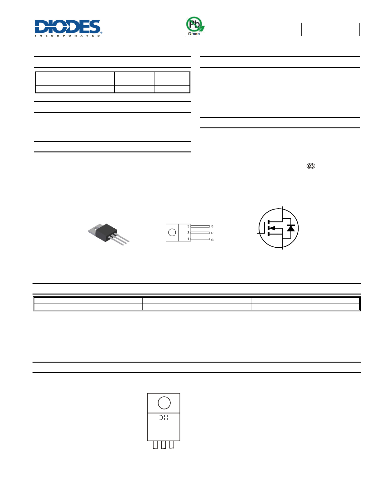
TO220-3
Top View
Features
I
D
TC = 25°C
• Low Input Capacitance
• High BVDss rating for power application
• Low Input/Output Leakage
• Lead-Free Finish; RoHS Compliant (Notes 1 & 2)
• Halogen and Antimony Free. “Green” Device (Note 3)
• Qualified to AEC-Q101 Standards for High Reliability
Mechanical Data
• Case: TO220-3
• Case Material: Molded Plastic, “Green” Molding Compound. UL
• Moisture Sensitivity: Level 1 per J-STD-020
• Terminals: Finish-Matte Tin annealed over Copper Leadframe
• Terminal Connections: See Diagram Below
• Weight: 0.008 grams (approximate)
Top View
Pin Out Configuration
DMG4N65CT
N-CHANNEL ENHANCEMENT MODE MOSFET
Flammability Classification Rating 94V-0
Solderable per MIL-STD-202, Method 208
D
G
S
Equivalent Circuit
Ordering Information (Note 4)
Part Number Case Packaging
DMG4N65CT TO220-3 50 pieces/tube
Notes: 1. EU Directive 2002/95/EC (RoHS) & 2011/65/EU (RoHS 2) compliant. All applicable RoHS exemptions applied.
2. See http://www.diodes.com for more information about Diodes Incorporated’s definitions of Halogen- and Antimony-free, "Green" and Lead-free.
3. Halogen- and Antimony-free "Green” products are defined as those which contain <900ppm bromine, <900ppm chlorine (<1500ppm total Br + Cl) and
<1000ppm antimony compounds.
4. For packaging details, go to our website at http://www.diodes.com.
Marking Information
4N65CT
YYWW
4N65CT = Product Type Marking Code
YYWW = Date Code Marking
YY = Last two digits of year (ex: 12 = 2012)
WW = Week (01 - 53)
DMG4N65CT
Document number: DS35719 Rev. 4 - 2
1 of 6
www.diodes.com
November 2012
© Diodes Incorporated

)
)
g
g
g
)
r
)
r
r
r
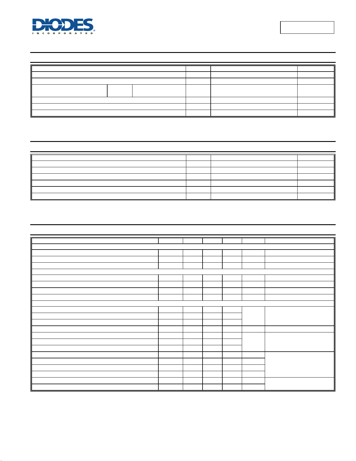
Maximum Ratings (@T
= +25°C, unless otherwise specified.)
A
Characteristic Symbol Value Unit
Drain-Source Voltage
Gate-Source Voltage
Continuous Drain Current (Note 5)
= 10V
V
GS
Steady
State
= +25°C
T
C
T
= +70°C
C
Pulsed Drain Current (Note 7)
Avalanche Current (Note 8) VDD = 100V, VGS = 10V, L = 60mH IAS
Repetitive avalanche energy (Note 7)
Thermal Characteristics
Characteristic Symbol Max Unit
Power Dissipation (Note 5)
Thermal Resistance, Junction to Ambient @TA = +25°C (Note 5) R
Power Dissipation (Note 6)
Thermal Resistance, Junction to Ambient @TA = +25°C (Note 6) R
Thermal Resistance, Junction to Case @TA = +25°C (Note 6) R
ADVANCE INFORMATIO
Operating and Storage Temperature Range
DMG4N65CT
V
DSS
V
GSS
I
D
I
DM
E
AS
P
D
θJA
P
D
θJA
θJC
T
, T
J
STG
650 V
±30 V
4.0
3.0
A
6 A
3.9 A
456 mJ
2.19 W
58.5 °C/W
9.14 W
2.85 °C/W
0.86 °C/W
-55 to +150 °C
Electrical Characteristics (@T
= +25°C, unless otherwise specified.)
A
Characteristic Symbol Min Typ Max Unit Test Condition
OFF CHARACTERISTICS (Note 9)
Drain-Source Breakdown Voltage
Zero Gate Voltage Drain Current TJ = 25°C I
Gate-Source Leakage
BV
I
DSS
DSS
GSS
650 - - V
- - 1.0
- - ±100 nA
VGS = 0V, ID = 250μA
μA
VDS = 650V, VGS = 0V
VGS = ±30V, VDS = 0V
ON CHARACTERISTICS (Note 9)
Gate Threshold Voltage
Static Drain-Source On-Resistance
Forward Transfer Admittance
Diode Forward Voltage
V
R
DS(ON
|Y
V
GS(th
fs
SD
|
3 - 5 V
- 2.1 3.0
- 3.7 - S
- 0.7 1.0 V
VDS = VGS, ID = 250μA
Ω
VGS = 10V, ID = 2A
VDS = 40V, ID = 2A
VGS = 0V, IS = 1A
DYNAMIC CHARACTERISTICS (Note 10)
Input Capacitance
Output Capacitance
Reverse Transfer Capacitance
Gate Resistance
C
iss
C
oss
C
rss
R
Total Gate Charge VGS = 10V Qg
Gate-Source Charge
Gate-Drain Charge
Turn-On Delay Time
Turn-On Rise Time
Turn-Off Delay Time
Turn-Off Fall Time
Body Diode Reverse Recovery Time
Notes: 5. Device mounted on FR-4 PCB with minimum recommended pad layout, single sided.
6. Device mounted on an infinite heatsink
7. Repetitive rating, pulse width limited by junction temperature.
8. I
and EAS rating are based on low frequency and duty cycles to keep TJ = +25°C.
AS
9. Short duration pulse test used to minimize self-heating effect.
10. Guaranteed by design. Not subject to production testing.
Q
Q
t
D(on
t
D(off
s
d
t
t
f
t
Q
r
- 900 -
-
-
-
13.5
-
-
-
15.1
-
13.8
-
-
515
-
2330
-
50
1.1
2.4
2.7
3.8
40
16
V
-
pF
-
-
Ω
-
-
nC
-
DS
f = 1.0MHz
VDS = 0V, VGS = 0V, f = 1MHz
V
GS
I
D
- ns
- ns
- ns
V
GS
R
G
- ns
- ns
- nC
dI/dt = 100A/μs, V
I
= 4A Body Diode Reverse Recovery Charge
F
= 25V, VGS = 0V,
= 10V, VDS = 520V,
= 4A
= 10V, VDS = 325V,
= 25Ω, ID = 4A
DS
= 100V,
DMG4N65CT
Document number: DS35719 Rev. 4 - 2
2 of 6
www.diodes.com
November 2012
© Diodes Incorporated
 Loading...