Diodes DMG4800LSD User Manual

Product Summary
I
max
D
9.8A
8.4A
V
(BR)DSS
30V
R
16m @ V
22m @ VGS = 4.5V
DS(on)
max
= 10V
GS
TA = +25°C
Description
This MOSFET has been designed to minimize the on-state resistance
(R
) and yet maintain superior switching performance, making it
DS(on)
ideal for high efficiency power management applications.
Applications
Backlighting
Power Management Functions
DC-DC Converters
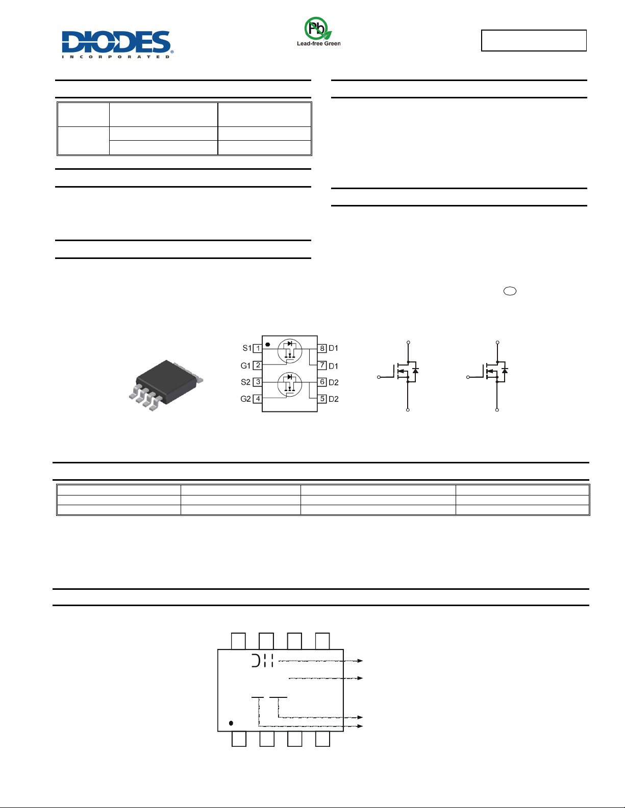
SO-8
Top View Pin Configuration
Top View
Internal Schematic
DMG4800LSD
DUAL N-CHANNEL ENHANCEMENT MODE MOSFET
Features and Benefits
100% avalanche rated part
Low R
Low Q
Totally Lead-Free & Fully RoHS Compliant (Notes 1 & 2)
Halogen and Antimony Free. “Green” Device (Note 3)
Qualified to AEC-Q101 standards for High Reliability
- minimizes conduction losses
DS(on)
- minimizes switching losses
g
Mechanical Data
Case: SO-8
Case Material: Molded Plastic, "Green" Molding Compound.
UL Flammability Classification Rating 94V-0
Moisture Sensitivity: Level 1 per J-STD-020
Terminal Connections Indicator: See diagram
Terminals: Finish Matte Tin annealed over Copper leadframe.
Solderable per MIL-STD-202, Method 208
Weight: 0.076 grams (approximate)
D
1
G
1
S
1
N-Channel MOSFET N-Channel MOSFET
G
2
e3
D
2
S
2
Ordering Information (Note 4)
Part Number Compliance Case Packaging
DMG4800LSD-13 Standard SO-8 2500 / Tape & Reel
DMG4800LSDQ-13 Automotive SO-8 2500 / Tape & Reel
Notes: 1. No purposely added lead. Fully EU Directive 2002/95/EC (RoHS) & 2011/65/EU (RoHS 2) compliant.
2. See http://www.diodes.com/quality/lead_free.html for more information about Diodes Incorporated’s definitions of Halogen- and Antimony-free, "Green"
and Lead-free.
3. Halogen- and Antimony-free "Green” products are defined as those which contain <900ppm bromine, <900ppm chlorine (<1500ppm total Br + Cl) and
<1000ppm antimony compounds.
4. For packaging details, go to our website at http”//www.diodes.com/products/packages.html.
Marking Information
DMG4800LSD
Document number: DS31858 Rev. 6 - 2
Top View
8 5
G4800LD
YY
WW
1 4
1 of 6
www.diodes.com
Logo
Part no.
Xth week: 01 ~ 53
Year: “10” = 2010
“11” = 2011
March 2013
© Diodes Incorporated

)
g
g
g
g
)
r
)
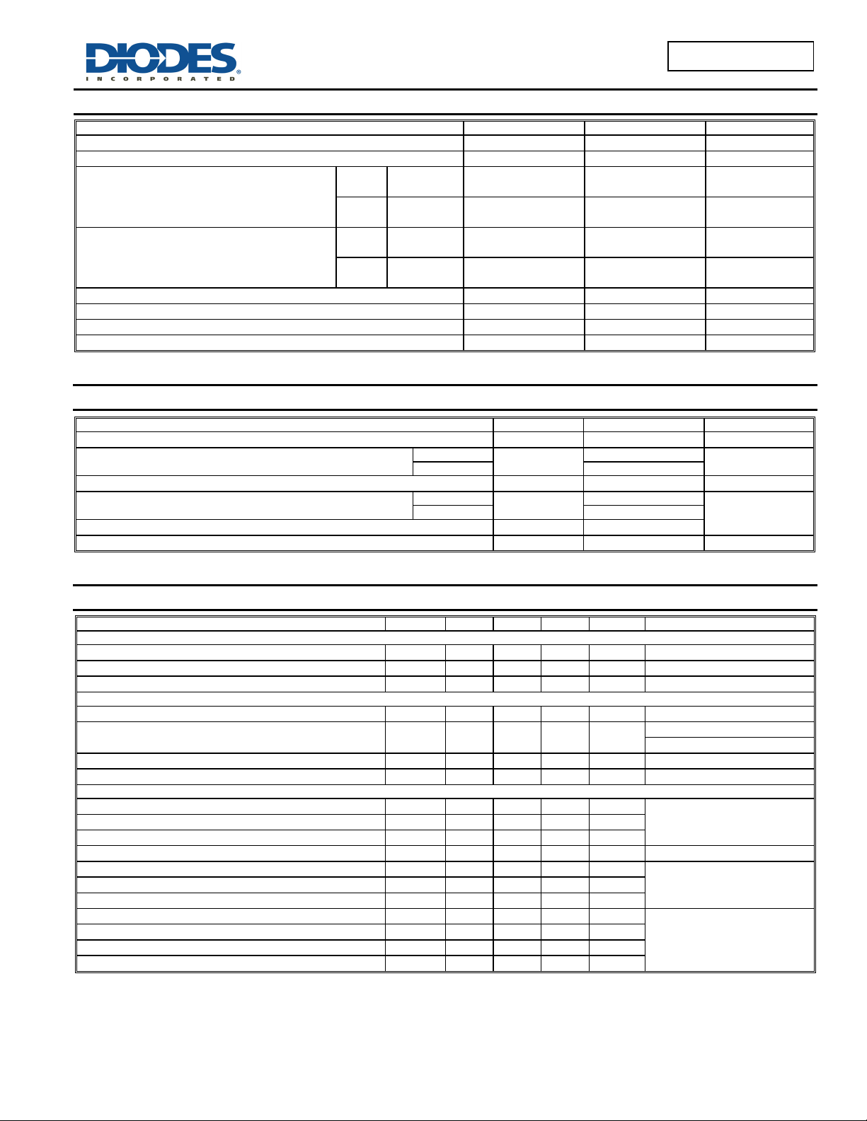
Maximum Ratings (@T
= +25°C, unless otherwise specified.)
A
Characteristic Symbol Value Units
Drain-Source Voltage
Gate-Source Voltage
Steady
Continuous Drain Current (Note 6) VGS = 10V
State
t<10s
Steady
Continuous Drain Current (Note 6) VGS = 4.5V
State
t<10s
Maximum Continuous Body Diode Forward Current (Note 6)
Pulsed Drain Current (10µs pulse, duty cycle = 1%)
Avalanche Current (Notes 7 & 8) L = 0.1mH
Repetitive Avalanche Energy (Notes 7 & 8) L = 0.1mH
Thermal Characteristics
Characteristic Symbol Value Units
Total Power Dissipation (Note 5)
Thermal Resistance, Junction to Ambient (Note 5)
Total Power Dissipation (Note 6)
Thermal Resistance, Junction to Ambient (Note 6)
Thermal Resistance, Junction to Case
Operating and Storage Temperature Range
DMG4800LSD
V
DSS
V
GSS
T
= +25°C
A
= +70°C
T
A
T
= +25°C
A
T
= +70°C
A
T
= +25°C
A
= +70°C
T
A
= +25°C
T
A
= +70°C
T
A
Steady State
t<10s 61
Steady State
t<10s 49
I
D
I
D
I
D
I
D
I
S
I
DM
I
AR
E
AR
T
J, TSTG
P
D
R
JA
P
D
R
JA
R
JC
30 V
±25 V
7.5
6.0
9.8
7.7
6.4
5.0
8.4
6.6
2 A
42 A
17 A
14 mJ
1.17 W
107
1.5 W
83
14.5
-55 to 150 °C
A
A
A
A
°C/W
°C/W
Electrical Characteristics (@T
= +25°C, unless otherwise specified.)
A
Characteristic Symbol Min Typ Max Unit Test Condition
OFF CHARACTERISTICS (Note 9)
Drain-Source Breakdown Voltage
Zero Gate Voltage Drain Current TJ = +25°C I
Gate-Source Leakage
BV
I
DSS
DSS
GSS
30 - - V
- - 1.0 A
- - ±100 nA
VGS = 0V, ID = 250A
VDS = 30V, VGS = 0V
VGS = ±20V, VDS = 0V
ON CHARACTERISTICS (Note 9)
Gate Threshold Voltage
Static Drain-Source On-Resistance
Forward Transfer Admittance
Diode Forward Voltage
V
R
GS(th
DS(on)
|Y
fs
V
SD
0.8 - 1.6 V
-
|
- 8 - S
- 0.72 0.94 V
12
16
16
22
VDS = VGS, ID = 250A
= 10V, ID = 9A
V
m
GS
VGS = 4.5V, ID = 7A
VDS = 10V, ID = 9A
VGS = 0V, IS = 1A
DYNAMIC CHARACTERISTICS (Note 10)
Input Capacitance
Output Capacitance
Reverse Transfer Capacitance
Gate Resistance
Total Gate Charge
Gate-Source Charge
Gate-Drain Charge
Turn-On Delay Time
Turn-On Rise Time
Turn-Off Delay Time
Turn-Off Fall Time
Notes: 5. Device mounted on FR-4 substrate PC board, 2oz copper, with minimum recommended pad layout.
6. Device mounted on FR-4 substrate PC board, 2oz copper, with 1inch square copper plate.
7. I
8. Applicable to products manufactured with Data Code “1146” (Nov, 2011) and newer.
9. Short duration pulse test used to minimize self-heating effect.
10. Guaranteed by design. Not subject to product testing.
and EAR rating are based on low frequency and duty cycles to keep TJ = +25°C.
AR
DMG4800LSD
Document number: DS31858 Rev. 6 - 2
C
iss
C
oss
C
rss
R
Q
Q
s
Q
d
t
D(on
t
t
D(off
t
f
www.diodes.com
- 798 - pF
- 128 - pF
- 122 - pF
- 1.37 -
- 8.56 - nC
- 1.8 - nC
- 2.5 - nC
- 5.03 - ns
- 4.50 - ns
- 26.33 - ns
- 8.55 - ns
2 of 6
V
= 10V, VGS = 0V,
DS
f = 1.0MHz
VDS = 0V, VGS = 0V, f = 1MHz
= 5V, VDS = 15V,
V
GS
I
= 9A
D
V
= 15V, V
DD
= 15, RG = 6, ID = 1A
R
L
= 10V,
GEN
March 2013
© Diodes Incorporated
 Loading...