

Diodes DMG4710SSS User Manual
N-CHANNEL ENHANCEMENT MODE MOSFET WITH SCHOTTKY DIODE
Product Summary
I
max
V
R
(BR)DSS
30V
DS(on)
12.5mΩ @ V
GS
= 10V
14.8mΩ @ VGS= 4.5V
D
TA = 25°C (Note 5)
11.7A
10.8A
Description and Applications
This new generation MOSFET has been designed to minimize the onstate resistance (R
performance, making it ideal for high efficiency power management
applications.
• DC-DC Converters
• Power management functions
) and yet maintain superior switching
DS(on)
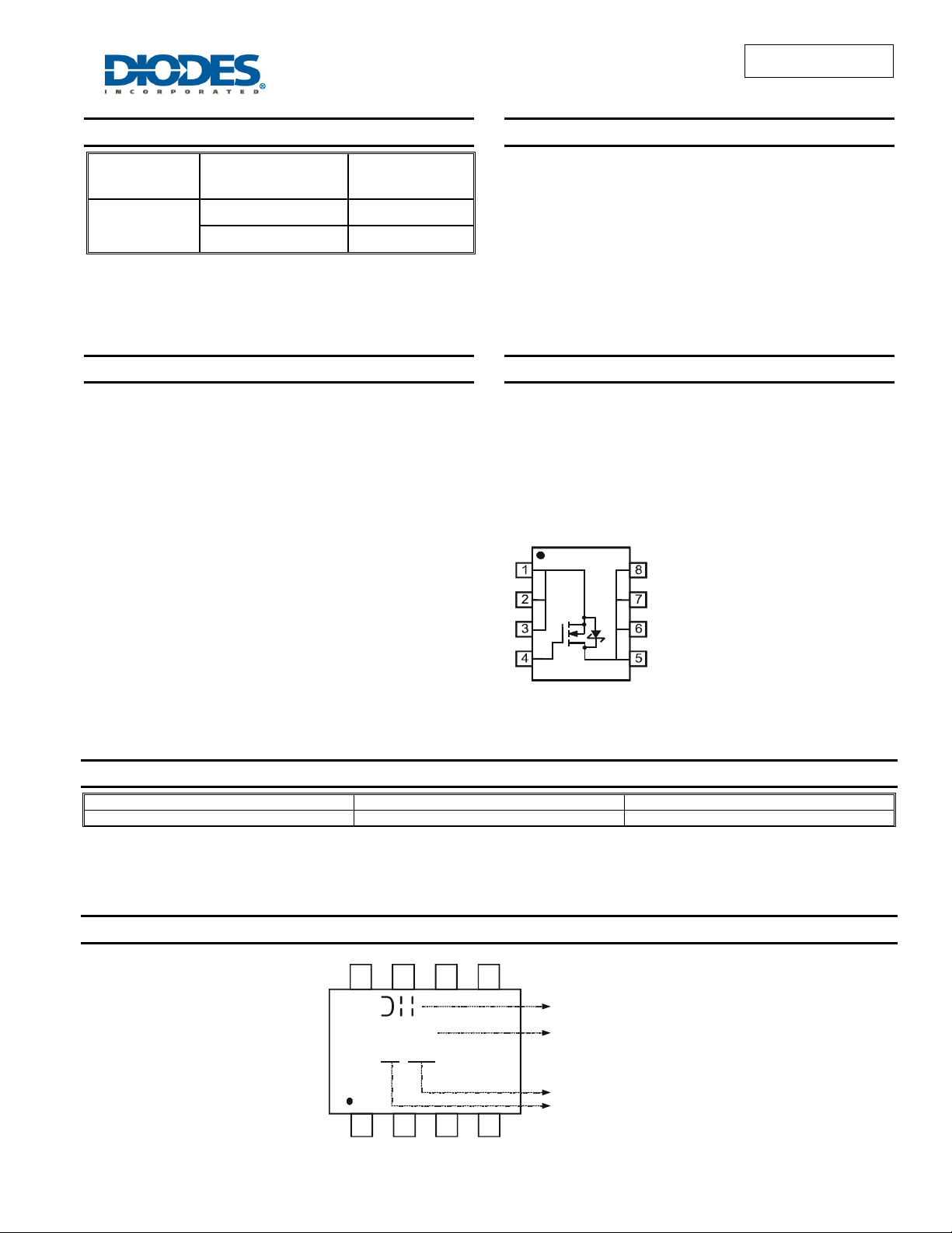
Top View
DMG4710SSS
Features
• DIOFET utilizes a unique patented process to monolithically
integrate a MOSFET and a Schottky in a single die to deliver:
• Low R
• Low V
• Low Q
- minimizes conduction losses
DS(ON)
- reducing the losses due to body diode conduction
SD
- lower Qrr of the integrated Schottky reduces body
rr
diode switching losses
• Low gate capacitance (Q
) ratio – reduces risk of shoot-
g/Qgs
through or cross conduction currents at high frequencies
• Avalanche rugged – I
and EAR rated
AR
• Lead Free, RoHS Compliant (Note 1)
• "Green" Device (Note 2)
• Qualified to AEC-Q101 Standards for High Reliability
Mechanical Data
• Case: SO-8
• Case Material: Molded Plastic, “Green” Molding Compound.
UL Flammability Classification Rating 94V-0
• Moisture Sensitivity: Level 1 per J-STD-020
• Terminal Connections: See Diagram Below
• Weight: 0.072 grams (approximate)
S
S
S
G
Top View
Internal Schematic
D
D
D
D
Ordering Information (Note 3)
Part Number Case Packaging
DMG4710SSS-13 SO-8 2500 / Tape & Reel
Notes: 1. No purposefully added lead.
2. Diodes Inc.'s "Green" policy can be found on our website at http://www.diodes.com.
3. For packaging details, go to our website at http://www.diodes.com.
Marking Information
DMG4710SSS
Document number: DS32055 Rev. 6 - 2
8 5
G4710SS
YY
WW
1 4
www.diodes.com
1 of 6
Logo
Part no.
Xth week: 01 ~ 53
Y ear: “09” = 2009
Y ear: “10” = 2010
November 2010
© Diodes Incorporated

)
g
g
g
)
r
)
Maximum Ratings @T
= 25°C unless otherwi se specified
A
Characteristic Symbol Value Unit
Drain-Source Voltage
Gate-Source Voltage
Continuous Drain Current (Note 4) VGS = 10V
Continuous Drain Current (Note 5) VGS = 10V
Continuous Drain Current (Note 5) VGS = 4.5V
Pulsed Drain Current (Note 6)
Avalanche Current (Notes 6 & 7)
Repetitive Avalanche Energy (Notes 6 & 7) L = 0.3mH
Thermal Characteristics
Characteristic Symbol Value Unit
Power Dissipation (Note 4)
Thermal Resistance, Junction to Ambient @T
Power Dissipation (Note 5)
Thermal Resistance, Junction to Ambient @T
Operating and Storage Temperature Range
= 25°C (Note 4) R
A
= 25°C (Note 5) R
A
Steady
State
t ≤ 10 sec
t ≤ 10 sec
A = 25°C
T
A = 85°C
T
A = 25°C
T
T
A = 85°C
A = 25°C
T
T
A = 85°C
DMG4710SSS
V
DSS
V
GSS
I
D
I
D
I
D
I
DM
IAR
E
AR
P
D
θJA
P
D
θJA
T
, T
J
STG
30 V
±12 V
8.8
6.3
11.7
8.5
10.8
7.8
A
A
A
90 A
13 A
25.4 mJ
1.54 W
81 °C/W
2.8 W
45 °C/W
-55 to +150 °C
Electrical Characteristics @ T
= 25°C unless otherwise stated
A
Characteristic Symbol Min Typ Max Unit Test Condition
OFF CHARACTERISTICS (Note 8)
Drain-Source Breakdown Voltage
Zero Gate Voltage Drain Current
Gate-Source Leakage
BV
I
DSS
I
GSS
DSS
30 - - V
- - 0.1 mA
- - ±100 nA
VGS = 0V, ID = 1mA
VDS = 30V, VGS = 0V
VGS = ±12V, VDS = 0V
ON CHARACTERISTICS (Note 8)
Gate Threshold Voltage
Static Drain-Source On-Resistance
Forward Transfer Admittance
Diode Forward Voltage
Maximum Body-Diode + Schottky Continuous Current
V
GS(th
R
DS (ON)
|Y
V
fs
SD
I
S
1.0 - 2.3 V
- 9.5 12.5
- 11.5 14.8
|
- 22 - S
- 0.38 0.6 V
- - 5 A -
VDS = VGS, ID = 250μA
= 10V, ID = 11.7A
V
mΩ
GS
V
= 4.5V, ID = 10.8A
GS
VDS = 5V, ID = 11.7A
VGS = 0V, IS = 1A
DYNAMIC CHARACTERISTICS (Note 9)
Input Capacitance
Output Capacitance
Reverse Transfer Capacitance
Gate Resistance
C
iss
C
oss
C
rss
R
Total Gate Charge VGS = 4.5V Qg
Total Gate Charge VGS = 10V Qg
Gate-Source Charge
Gate-Drain Charge
Turn-On Delay Time
Turn-On Rise Time
Turn-Off Delay Time
Turn-Off Fall Time
Notes: 4. Device mounted on FR-4 PCB with minimum recommended pad layout. The value in any given application depends on the user’s specific board design.
5. Device mounted on 1” x 1” FR-4 PCB with high coverage 1 oz. Copper, single sided , device is measured at t ≤ 10 sec.
6. Repetitive rating, pulse width limited by junction temperature.
and EAR rating are based on low frequency and duty cycles to keep TJ = 25°C
7. I
AR
8. Short duration pulse test used to minimize self-heating effect.
9. Guaranteed by design. Not subject to production testing.
Q
Q
t
D(on
t
D(off
s
d
t
t
f
- 1849 - pF
- 158 - pF
- 123 - pF
0.54 2.68 4.82
- 18.5 - nC
- 43 - nC
- 4.7 - nC
- 4.0 - nC
- 6.62 - ns
- 8.73 - ns
- 36.41 - ns
- 4.69 - ns
V
=15V, VGS = 0V,
DS
f = 1.0MHz
Ω
VDS =0V, VGS = 0V, f = 1MHz
V
= 15V, VGS = 10V,
DS
= 11.7A
I
D
V
= 10V, VDS = 10V,
GS
= 3Ω, RL = 1.2Ω
R
G
DMG4710SSS
Document number: DS32055 Rev. 6 - 2
2 of 6
www.diodes.com
November 2010
© Diodes Incorporated
 Loading...