

Page 1
Product Summary
I
V
R
(BR)DSS
35V 35m @ VGS = 10V 13A
-35V 45m @ VGS = -10V -12A
DS(ON)
D
TA = 25°C
Description and Applications
This new generation MOSFET has been designed to minimize the onstate resistance (R
performance, making it ideal for high efficiency power management
applications.
• Backlighting
• DC-DC Converters
• Power management functions
) and yet maintain superior switching
DS(on)
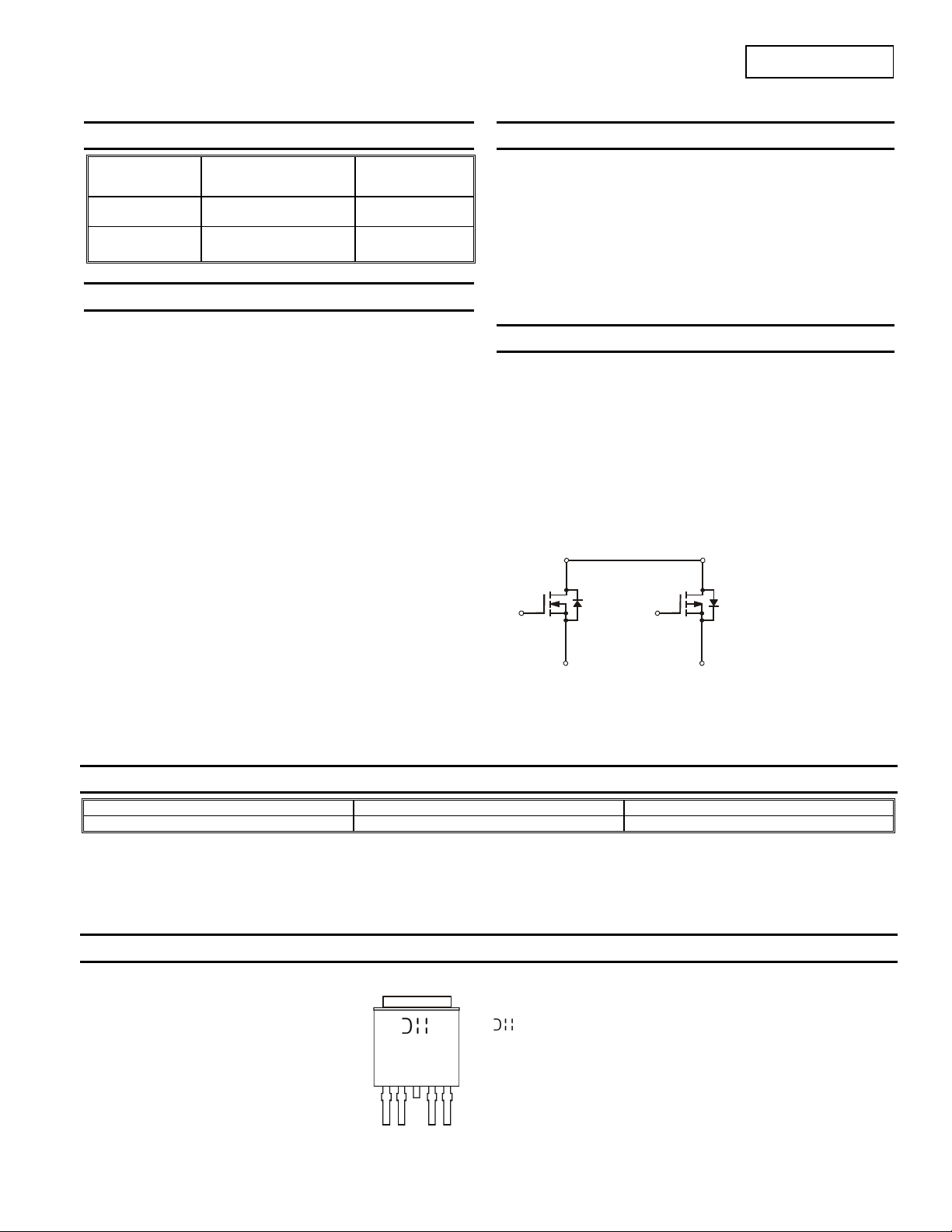
Top View
Bottom View
DMG4511SK4
COMPLEMENTARY PAIR ENHANCEMENT MODE MOSFET
Features and Benefits
• Low On-Resistance
• Low Gate Threshold Voltage
• Low Input Capacitance
• Fast Switching Speed
• Low Input/Output Leakage
• Complementary Pair MOSFET
• Lead Free/RoHS Compliant (Note 1)
• "Green" Device (Note 2)
• Qualified to AEC-Q101 Standards for High Reliability
Mechanical Data
• Case: TO252-4L
• Case Material: Molded Plastic, “Green” Molding Compound. UL
Flammability Classification Rating 94V-0
• Moisture Sensitivity: Level 1 per J-STD-020
• Terminal Connections: See Diagram Below
• Terminals: Finish – Matte Tin annealed over Copper leadframe.
Solderable per MIL-STD-202, Method 208
• Weight: 0.328 grams (approximate)
D
2
G
2
S
2
N-Channel MOSFE T P-Channel MOSF ET
G
1
D
1
S
1
Ordering Information (Note 3)
Part Number Case Packaging
DMG4511SK4-7 TO252-4L 3000 / Tape & Reel
Notes: 1. No purposefully added lead.
2. Diodes Inc.'s "Green" policy can be found on our website at http://www.diodes.com.
3. For packaging details, go to our website at http://www.diodes.com.
Marking Information
DMG4511SK4
Document number: DS32042 Rev. 4 - 2
G4511S
YYWW
= Manufacturer’s Marking
G4511S = Product Type Marking Code
YYWW = Date Code Marking
YY = Year (ex: 09 = 2009)
WW = Week (01 – 53)
1 of 9
www.diodes.com
July 2011
© Diodes Incorporated
Page 2
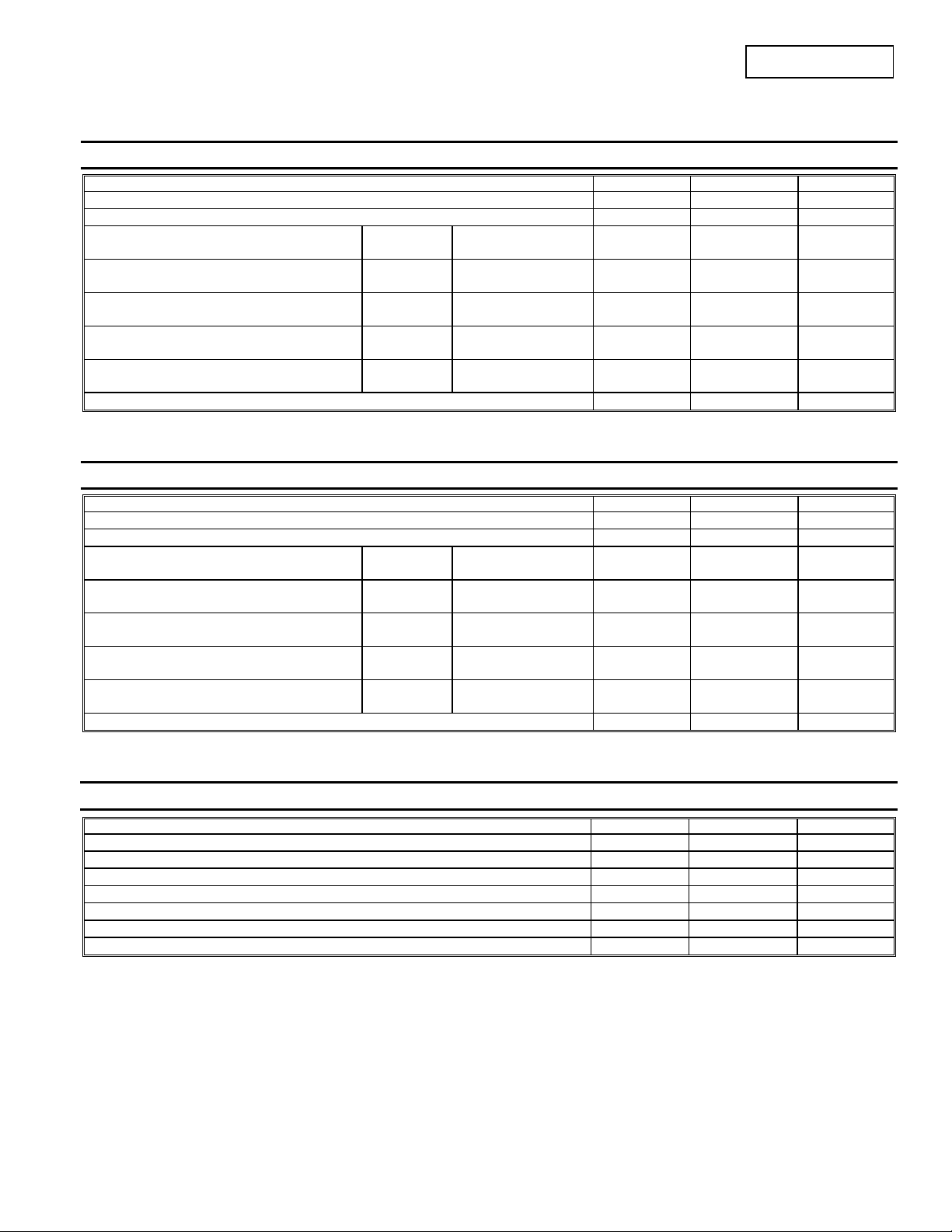
Maximum Ratings – N-CHANNEL, Q1 @T
Characteristic Symbol Value Unit
Drain-Source Voltage
Gate-Source Voltage
Continuous Drain Current (Note 4) VGS = 10V
Continuous Drain Current (Note 5) VGS = 10V
Continuous Drain Current (Note 5) VGS = 10V
Continuous Drain Current (Note 5) VGS = 4.5V
Continuous Drain Current (Note 5) VGS = 4.5V
Steady
State
Steady
State
t 10s
Steady
State
t 10s
Pulsed Drain Current (Note 6)
Maximum Ratings – P-CHANNEL, Q2 @T
Characteristic Symbol Value Unit
Drain-Source Voltage
Gate-Source Voltage
Continuous Drain Current (Note 4) VGS = -10V
Continuous Drain Current (Note 5) VGS = -10V
Continuous Drain Current (Note 5) VGS = -10V
Continuous Drain Current (Note 5) VGS = -4.5V
Continuous Drain Current (Note 5) VGS = -4.5V
Pulsed Drain Current (Note 6)
Steady
State
Steady
State
t 10s
Steady
State
t 10s
= 25°C unless otherwise specified
A
V
V
T
= 25°C
A
= 70°C
T
A
T
= 25°C
A
T
= 70°C
A
= 25°C
T
A
T
= 70°C
A
T
= 25°C
A
= 70°C
T
A
= 25°C
T
A
T
= 70°C
A
= 25°C unless otherwise specified
A
V
V
T
= 25°C
A
T
= 70°C
A
T
= 25°C
A
= 70°C
T
A
T
= 25°C
A
T
= 70°C
A
T
= 25°C
A
= 70°C
T
A
= 25°C
T
A
= 70°C
T
A
DSS
GSS
I
I
I
I
I
I
DM
DSS
GSS
I
I
I
I
I
I
DM
DMG4511SK4
D
D
D
D
D
D
D
D
D
D
35 V
±20 V
5.3
4.2
8.6
6.8
13
11
6.3
5.0
9.3
7.4
A
A
A
A
A
50 A
-35 V
±20 V
-5.0
-3.8
-7.8
-6.2
-12
-10
-6.5
-5.2
-9.6
-7.7
A
A
A
A
A
-50 A
Thermal Characteristics
Characteristic Symbol Value Unit
Power Dissipation (Note 4)
Thermal Resistance, Junction to Ambient @TA = 25°C (Note 4) R
Power Dissipation (Note 5)
Thermal Resistance, Junction to Ambient @TA = 25°C (Note 5) R
Power Dissipation (Note 5) t 10s
Thermal Resistance, Junction to Ambient @TA = 25°C (Note 5) t 10s R
Operating and Storage Temperature Range
Notes: 4. Device mounted on FR-4 PCB with minimum recommended pad layout, single sided.
5. Device mounted on 2” x 2” FR-4 PCB with high coverage 2 oz. Copper, single sided.
6. Repetitive rating, pulse width limited by junction temperature.
DMG4511SK4
Document number: DS32042 Rev. 4 - 2
2 of 9
www.diodes.com
P
D
JA
P
D
JA
P
D
JA
, T
T
J
STG
1.54 W
81.3
°C/W
4.1 W
30.8
°C/W
8.9 W
14
°C/W
-55 to +150 °C
July 2011
© Diodes Incorporated
Page 3
)
g
g
g
r
)
g
g
g
)
r
)
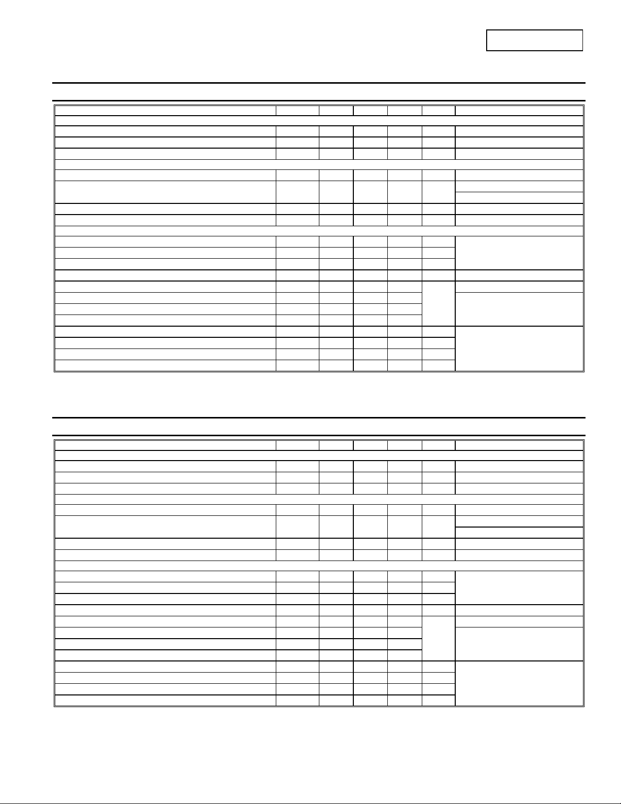
Electrical Characteristics – N-CHANNEL, Q1 @T
OFF CHARACTERISTICS (Note 7)
Drain-Source Breakdown Voltage
Zero Gate Voltage Drain Current TJ = 25°C I
Gate-Source Leakage
ON CHARACTERISTICS (Note 7)
Gate Threshold Voltage
Static Drain-Source On-Resistance
Forward Transfer Admittance
Diode Forward Voltage
DYNAMIC CHARACTERISTICS (Note 8)
Input Capacitance
Output Capacitance
Reverse Transfer Capacitance
Gate Resistance
Total Gate Charge (VGS = 10V) Qg
Total Gate Charge (VGS = 4.5V) Qg
Gate-Source Charge
Gate-Drain Charge
Turn-On Delay Time
Turn-On Rise Time
Turn-Off Delay Time
Turn-Off Fall Time
Characteristic Symbol Min Typ Max Unit Test Condition
BV
DSS
DSS
I
GSS
V
GS(th
R
DS (ON)
|Y
|
fs
V
SD
C
iss
C
oss
C
rss
R
Q
s
Q
d
t
D(on)
t
t
D(off)
t
f
= 25°C unless otherwise specified
A
35 - - V
- - 1.0
μA
- - ±100 nA
1.0 - 3.0 V
-
25
50
35
65
mΩ
- 4.5 - S
- - 1.2 V
- 850 - pF
- 64.7 - pF
- 51.9 - pF
- 1.6 -
Ω
- 18.7 -
- 8.8 -
- 2.6 -
nC
- 2.1 -
- 5.4 - ns
- 2.8 - ns
- 33.2 - ns
- 35.6 - ns
DMG4511SK4
VGS = 0V, ID = 250A
VDS = 35V, VGS = 0V
VGS = ±20V, VDS = 0V
VDS = VGS, ID = 250A
= 10V, ID = 8A
V
GS
VGS = 4.5V, ID = 6A
VDS = 10V, ID = 8A
VGS = 0V, IS = 8A
V
= 25V, VGS = 0V,
DS
f = 1.0MHz
VDS = 0V, VGS = 0V, f = 1MHz
VGS = 10V, VDS = 28V, ID = 8A
V
= 4.5V, VDS = 28V,
GS
I
= 8A
D
= 18V, VGS = 10V,
V
DS
R
= 18, RG = 3.3,
L
= 1A
I
D
Electrical Characteristics – P-CHANNEL, Q2 @T
= 25°C unless otherwise specified
A
Characteristic Symbol Min Typ Max Unit Test Condition
OFF CHARACTERISTICS (Note 7)
Drain-Source Breakdown Voltage
Zero Gate Voltage Drain Current TJ = 25°C I
Gate-Source Leakage
BV
DSS
I
GSS
DSS
-35 - - V
- - -1.0
- - ±100 nA
VGS = 0V, ID = -250A
μA
VDS = -35V, VGS = 0V
VGS = ±20V, VDS = 0V
ON CHARACTERISTICS (Note 7)
Gate Threshold Voltage
Static Drain-Source On-Resistance
Forward Transfer Admittance
Diode Forward Voltage
V
GS(th
R
DS (ON)
|Y
V
fs
SD
-1.0 - -3.0 V
-
|
- 8 - S
30
40
- -1.2 V
45
65
VDS = VGS, ID = -250A
= -10V, ID = -6A
V
mΩ
GS
VGS = -4.5V, ID = -4A
VDS = -10V, ID = -6A
VGS = 0V, IS = -6A
DYNAMIC CHARACTERISTICS (Note 8)
Input Capacitance
Output Capacitance
Reverse Transfer Capacitance
Gate Resistance
C
iss
C
oss
C
rss
R
Total Gate Charge (VGS = -10V) Qg
Total Gate Charge (VGS = -4.5V) Qg
Gate-Source Charge
Gate-Drain Charge
Turn-On Delay Time
Turn-On Rise Time
Turn-Off Delay Time
Turn-Off Fall Time
Notes: 7. Short duration pulse test used to minimize self-heating effect.
8. Guaranteed by design. Not subject to production testing.
DMG4511SK4
Document number: DS32042 Rev. 4 - 2
Q
s
Q
d
t
D(on
t
t
D(off
t
f
www.diodes.com
- 985.2 - pF
- 90.6 - pF
- 75.3 - pF
- 7.0 -
- 19.2 -
- 9.5 -
- 2.0 -
- 3.5 -
- 5.2 - ns
- 4.8 - ns
- 45.8 - ns
- 29.5 - ns
3 of 9
= -25V, VGS = 0V,
V
DS
f = 1.0MHz
Ω
VDS = 0V, VGS = 0V, f = 1MHz
VGS = -10V, VDS = -28V, ID = -6A
nC
V
= -4.5V, VDS = -28V,
GS
I
= -6A
D
= -18V, VGS = -10V,
V
DS
= 18, RG = 3.3,
R
L
I
= -1A
D
© Diodes Incorporated
July 2011
Page 4

R
CUR
RENT
R
C
URRENT
R
R
OUR
CE ON-R
TANC
R
R
OUR
CE ON-R
TANC
DMG4511SK4
N-CHANNEL, Q1
30
V = 8.0V
V = 4.5V
GS
V = 4.0V
GS
GS
V = 3.5V
GS
(A)
25
20
15
AIN
10
D
I, D
5
0
0 0.5 1 1.5 2
V , DRAIN-SOURCE VOLTAGE (V)
DS
V = 3.2V
GS
V = 3.0V
GS
V = 2.8V
GS
Fig. 1 Typica l O ut put Chara ct er istic
0.05
Ω
E ( )
0.04
ESIS
0.03
V = 4.5V
GS
V = 8.0V
GS
0.02
AIN-S
0.01
, D
DS(ON)
0
0 5 10 15 20 25 30
I , DRAIN-SOURCE CURRENT (A)
D
Fig. 3 Typical On-Resistance
vs. Drain C urrent an d G at e Vol t age
1.7
V = 10V
1.5
GS
I = 10A
D
30
V = 5V
DS
25
(A)
20
15
AIN
10
D
I, D
5
0
012345
V , GATE- SOURCE VOLTAGE (V)
GS
Fig. 2 Typical Transfer Characteristic
0.08
Ω
E ( )
0.07
V = 4.5V
GS
0.06
ESIS
T = 150°C
A
T = 125°C
A
T = 85°C
A
T = 25°C
A
T = -55°C
A
T = 150°C
A
0.05
T = 125°C
A
AIN-S
0.04
0.03
0.02
T = 85°C
A
T = 25°C
A
T = -55°C
A
, D
0.01
DS(ON)
0
0 5 10 15 20 25 30
I , DRAIN CURRENT (A)
D
Fig. 4 Typical On-Resistance
vs. Drain C urrent and Temperature
0.06
Ω
0.05
1.3
1.1
0.9
DSON
R , DRAIN-SOURCE
0.7
ON-RESISTANCE (NORMALIZED)
0.5
-50 -25 0 25 50 75 100 125 150
T , AMBIENT TEMPERATURE (°C)
A
Fig. 5 On-Resistance V ariation with Temperature
V = 4.5V
GS
I = 5A
D
0.04
V = 4.5V
GS
I = 5A
D
0.03
V = 10V
0.02
GS
I = 10A
D
0.01
DSON
R , DRAIN-SOURCE ON-RESISTANCE ( )
0
-50 -25 0 25 50 75 100 125 150
T , AMBIENT TEMPERATURE (°C)
A
Fig. 6 On-Resistance Variation with Temperature
DMG4511SK4
Document number: DS32042 Rev. 4 - 2
4 of 9
www.diodes.com
July 2011
© Diodes Incorporated
Page 5

OUR
CE CUR
REN
T
C, CAPACITANC
F
GE CUR
RENT
T
R
T T
HER
R
TANC
DMG4511SK4
3.0
2.7
2.4
2.1
1.8
1.5
I = 250µA
D
1.2
0.9
0.6
GS(TH)
0.3
V , GATE THRESHOLD VOLT AGE (V)
0
-50 -25 0 25 50 75 100 125 150
Fig. 7 Gat e Threshold V ariation vs. Ambient Temperature
T , AMBIENT TEMPERATURE (°C)
A
1,400
1,200
)
1,000
E (p
800
C
iss
f = 1MHz
20
18
16
14
(A)
T = 25°C
A
12
10
8
6
S
I, S
4
2
0
0.2 0.4 0.6 0.8 1.0 1.2
V , SOURCE-DRAIN VOLTAGE (V)
SD
Fig. 8 Diode Forward Voltage vs. Current
10,000
(nA )
1,000
T = 150°C
A
T = 125°C
A
100
600
T = 85°C
A
400
200
C
oss
C
rss
0
0 5 10 15 20 25 30 35
V , DRAIN-SOURCE VOLTAGE (V)
DS
Fig. 9 Typica l Total Capacitance
10
DSS
I , LEAKA
1
5101520253035
V , DRAIN-SOURCE VOLTAGE (V)
DS
Fig. 10 Typical Leakage Current
vs. Drain-S ource Voltage
T = 25°C
A
1
E
D = 0.7
D = 0.5
D = 0.3
ESIS
0.1
D = 0.1
MAL
D = 0.05
D = 0.02
0.01
D = 0.01
ANSIEN
D = 0.005
r(t),
D = Single Pulse
0.001
0.00001 0.0001
0.001 0.01 0.1 1 10 100 1,000
t , PULSE DURATION TIME (s)
D = 0.9
R (t) = r(t) *
θ
JA
R = 80°C/W
P(pk)
T - T = P * R (t)
JA JA12θ
Duty Cycle, D = t /t
1
R
JA
t
θθJA
1
t
2
Fig. 11 Transient Thermal Response
DMG4511SK4
Document number: DS32042 Rev. 4 - 2
5 of 9
www.diodes.com
July 2011
© Diodes Incorporated
Page 6

R
CUR
RENT
RAIN CUR
REN
T
R
RAIN-SOUR
CE O
N-R
TAN
C
R
RAIN-SOUR
CE O
N-R
TAN
C
R
RAIN
O
U
R
CE O
N
R
T
N
C
DMG4511SK4
P-CHANNEL, Q2
30
V = -8.0V
GS
25
(A)
20
15
AIN
10
D
-I , D
5
V = -2.8V
0
0 0.5 1 1.5 2
-V , DRAIN-SOURCE VOLTAGE (V)
DS
Fig. 12 Typical Output Characteristic
0.08
Ω
E ( )
0.07
GS
0.06
ESIS
0.05
V = -4.5V
0.04
0.03
GS
V = -8.0V
GS
0.02
, D
0.01
DS(ON)
0
0 5 10 15 20 25 30
-I , DRAIN-SOURCE CURRENT (A)
D
Fig. 14 Typical On-Resistance
vs. Drain C urrent and G ate V ol tage
1.7
1.5
1.3
1.1
V = -10V
GS
I = -10A
D
0.9
DSON
R , DRAIN-SOURCE
ON-RESISTANCE (NORMALIZED)
0.7
0.5
V = -4.5V
GS
I = -5A
D
-50 -25 0 25 50 75 100 125 150
T , AMBIENT TEMPERATURE (°C)
A
Fig. 16 On-Resistance Variation with Temperature
V = -4.5V
GS
V = -4.0V
GS
V = -3.5V
GS
V = -3.2V
GS
V = -3.0V
GS
30
25
(A)
20
15
10
D
-I , D
5
0
012345
0.10
Ω
T = 150°C
A
T = 125°C
A
-V , GATE-SOURCE VOLTAGE (V)
GS
Fig. 13 Typical Transfer Characteristic
T = 85°C
A
T = 25°C
A
T = -55°C
A
E ( )
0.08
ESIS
0.06
0.04
0.02
, D
DS(ON)
0
0 5 10 15 20 25 30
T = 150°C
A
T = 125°C
A
T = 85°C
A
T = 25°C
A
T = -55°C
A
-I , DRAIN CURRENT (A)
D
Fig. 15 Typical On-Resistan ce
vs. Drain C urrent and Temperature
0.10
Ω
0.09
E ( )
0.08
A
0.07
ESIS
-
0.06
V = -4.5V
0.05
GS
I = -5A
D
0.04
-S
0.03
0.02
, D
0.01
DSON
0
-50 -25 0 25 50 75 100 125 150
T , AMBIENT TEMPERATURE (°C)
Fig. 17 On-Resistance V ariation with Temperature
A
V = -10V
GS
I = -10A
D
DMG4511SK4
Document number: DS32042 Rev. 4 - 2
6 of 9
www.diodes.com
July 2011
© Diodes Incorporated
Page 7

OUR
CE CUR
RENT
C, TOT
CAPACITANC
F
GE CUR
RENT
T
R
T
T
HER
R
TANC
DMG4511SK4
3.0
2.7
2.4
2.1
1.8
1.5
I = -250µA
D
1.2
0.9
0.6
GS(TH)
0.3
-V , GATE THRESHOLD VOLTAGE (V)
0
-50 -25 0 25 50 75 100 125 150
T , AMBIENT TEMPERATURE (°C)
A
Fig. 18 Gat e Threshold Varia t ion vs. Ambien t Temperatur e
1,400
20
18
16
(A)
14
12
T = 25°C
A
10
8
6
S
-I , S
4
2
0
0.2 0.4 0.6 0.8 1.0 1.2
-V , SOURCE-DRAIN VOLTAGE (V)
SD
Fig. 19 Diode Forward Voltage vs. Current
10,000
f = 1MHz
(nA)
1,000
T = 150°C
A
T = 125°C
A
)
E (p
1,200
1,000
800
C
iss
100
600
AL
400
T
C
200
0
oss
C
rss
0 5 10 15 20 25 30 35
-V , DRAIN-SOURCE VOLTAGE (V)
DS
Fig. 20 Typical Total Capacitance
10
DSS
-I , LEAKA
1
5101520253035
-V , DRAIN-SOURCE VOLTAGE (V)
DS
Fig. 21 Typical Leakage Current vs. Drain-Source Voltage
T = 85°C
A
T = 25°C
A
1
E
D = 0.7
D = 0.5
D = 0.3
ESIS
0.1
D = 0.1
MAL
D = 0.05
D = 0.02
0.01
D = 0.01
ANSIEN
D = 0.005
r(t),
D = Single Pulse
0.001
0.00001 0.0001 0.001 0.01 0.1 1 10 100 1,000
t , PULSE DURATION TIME (s)
1
D = 0.9
R (t) = r(t) *
θ
JA
R = 80°C/W
JA
θ
P(pk)
t
1
t
2
T - T = P * R (t)
JA JA
Duty Cycle, D = t /t
R
θ
JA
θ
12
Fig. 22 T ransient Thermal Response
DMG4511SK4
Document number: DS32042 Rev. 4 - 2
7 of 9
www.diodes.com
July 2011
© Diodes Incorporated
Page 8

Package Outline Dimensions
4X b2
E
b3
L3
D
L4
e
5X b
Suggested Pad Layout
Y1
X1
c1
X (4x)
DMG4511SK4
TO252-4L
Dim Min Max Typ
A
c2
A2
H
A1
L
a
Y2
Y3
Y
c
E1
Dimensions Value (in mm)
c 1.27
c1 2.54
X 1.00
X1 5.73
Y 2.00
Y1 6.17
Y2 1.64
Y3 2.66
A 2.19 2.39 2.29
A1 0.00 0.13 0.08
A2 0.97 1.17 1.07
b 0.51 0.71 0.583
b2 0.61 0.79 0.70
b3 5.21 5.46 5.33
c2 0.45 0.58 0.531
D 6.00 6.20 6.10
D1 5.21
e
E 6.45 6.70 6.58
E1 4.32
H 9.40 10.41 9.91
L 1.40 1.78 1.59
L3 0.88 1.27 1.08
L4 0.64 1.02 0.83
a 0° 10°
All Dimensions in mm
− −
− −
1.27
− −
−
DMG4511SK4
Document number: DS32042 Rev. 4 - 2
8 of 9
www.diodes.com
July 2011
© Diodes Incorporated
Page 9

IMPORTANT NOTICE
DIODES INCORPORATED MAKES NO WARRANTY OF ANY KIND, EXPRESS OR IMPLIED, WITH REGARDS TO THIS DOCUMENT,
INCLUDING, BUT NOT LIMITED TO, THE IMPLIED WARRANTIES OF MERCHANTABILITY AND FITNESS FOR A PARTICULAR PURPOSE
(AND THEIR EQUIVALENTS UNDER THE LAWS OF ANY JURISDICTION).
Diodes Incorporated and its subsidiaries reserve the right to make modifications, enhancements, improvements, corrections or other changes
without further notice to this document and any product described herein. Diodes Incorporated does not assume any liability arising out of the
application or use of this document or any product described herein; neither does Diodes Incorporated convey any license under its patent or
trademark rights, nor the rights of others. Any Customer or user of this document or products described herein in such applications shall assume
all risks of such use and will agree to hold Diodes Incorporated and all the companies whose products are represented on Diodes Incorporated
website, harmless against all damages.
Diodes Incorporated does not warrant or accept any liability whatsoever in respect of any products purchased through unauthorized sales channel.
Should Customers purchase or use Diodes Incorporated products for any unintended or unauthorize d application, Customers shall indemnify and
hold Diodes Incorporated and its representatives harmless against all claims, damages, expenses, and attorney fees arising out of, directly or
indirectly, any claim of personal injury or death associated with such unintended or unauthorized application.
Products described herein may be covered by one or more United States, international or foreign patents pending. Product names and markings
noted herein may also be covered by one or more United States, international or foreign trademarks.
LIFE SUPPORT
Diodes Incorporated products are specifically not authorized for use as critical components in life support devices or systems without the express
written approval of the Chief Executive Officer of Diodes Incorporated. As used herein:
A. Life support devices or systems are devices or systems which:
1. are intended to implant into the body, or
2. support or sustain life and whose failure to perform when properly used in accordance with instructions for use provided in the
labeling can be reasonably expected to result in significant injury to the user.
B. A critical component is any component in a life support device or system whose failure to perform can be reasonably expected to cause the
failure of the life support device or to affect its safety or effectiveness.
Customers represent that they have all necessary expertise in the safety and regulatory ramifications of their life support devices or systems, and
acknowledge and agree that they are solely responsible for all legal, regulatory and safety-related requirements concerning their products and any
use of Diodes Incorporated products in such safety-critical, life support devices or systems, notwithstanding any devices- or systems-related
information or support that may be provided by Diodes Incorporated. Further, Customers must fully indemnify Diodes Incorporated and its
representatives against any damages arising out of the use of Diodes Incorporated products in such safety-critical, life support devices or systems.
Copyright © 2011, Diodes Incorporated
www.diodes.com
DMG4511SK4
DMG4511SK4
Document number: DS32042 Rev. 4 - 2
9 of 9
www.diodes.com
July 2011
© Diodes Incorporated
 Loading...