

Diodes DMG3415UFY4 User Manual
Please click here to visit our online spice models database.
Features
• Low On-Resistance
• 39mΩ @ V
• 52mΩ @ V
• 65mΩ @ V
• Low Input Capacitance
• Fast Switching Speed
• Low Input/Output Leakage
• Lead Free By Design/RoHS Compliant (Note 1)
• ESD Protected Up To 3kV
• "Green" Device, Halogen and Antimony Free (Note 2)
• Qualified to AEC-Q101 Standards for High Reliability
NEW PRODUCT
= -4.5V
GS
= -2.5V
GS
= -1.8V
GS
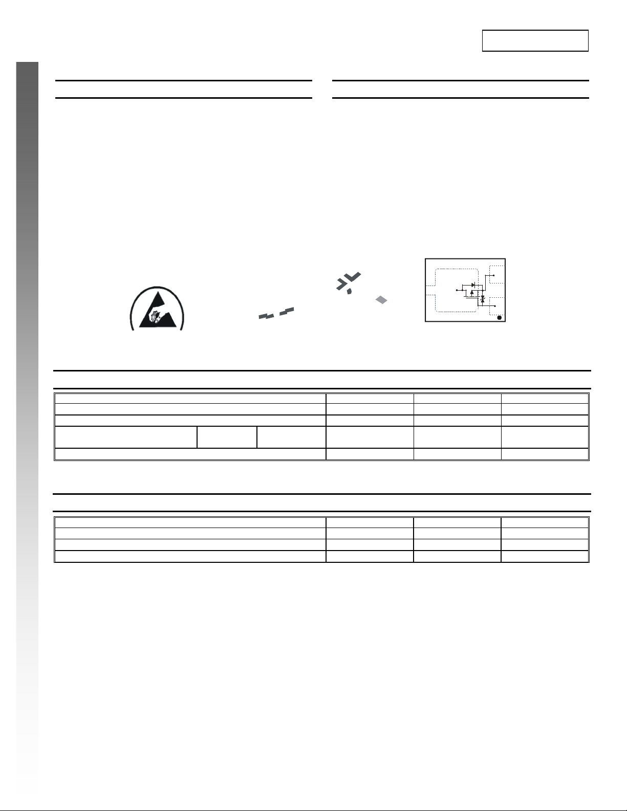
ESD PROTECTED TO 3kV
TOP VIEW
DMG3415UFY4
P-CHANNEL ENHANCEMENT MODE MOSFET
Mechanical Data
• Case: DFN2015H4-3
• Case Material: Molded Plastic, “Green” Molding Compound.
UL Flammability Classification Rating 94V-0
• Moisture Sensitivity: Level 1 per J-STD-020
• Terminals: Finish ⎯ Matte Tin over Copper leadframe.
Solderable per MIL-STD-202, Method 208
• Terminals Connections: See Diagram Below
• Marking Information: See Page 4
• Ordering Information: See Page 4
• Weight: 0.008 grams (approximate)
S
D
G
BOTTOM VIEW
Internal Schematic
Maximum Ratings @T
= 25°C unless otherwise specified
A
Characteristic Symbol Value Units
Drain-Source Voltage
Gate-Source Voltage
Continuous Drain Current (Note 3)
Steady
State
Pulsed Drain Current (Note 4)
Thermal Characteristics
Characteristic Symbol Value Unit
Power Dissipation (Note 3)
Thermal Resistance, Junction to Ambient @TA = 25°C R
Operating and Storage Temperature Range
Notes: 1. No purposefully added lead.
2. Diodes Inc.'s "Green" policy can be found on our website at http://www.diodes.com/products/lead_free/index.php.
3. Device mounted on FR-4 PCB with 2oz. Copper and test pulse width t ≤ 10s.
4. Repetitive rating, pulse width limited by junction temperature.
DMG3415UFY4
Document number: DS31842 Rev. 4 - 2
T
= 25°C
A
T
= 70°C
A
1 of 6
www.diodes.com
V
V
I
P
T
J, TSTG
DSS
GSS
I
D
DM
D
θJA
-16 V
±8 V
-2.5
-2.2
A
-12 A
0.49 W
250.7 °C/W
-55 to +150 °C
December 2009
© Diodes Incorporated
)
g
g
g
g
)
r
)
R
CUR
R
T
R
N
CUR
REN
T
Electrical Characteristics @T
= 25°C unless otherwise specified
A
Characteristic Symbol Min Typ Max Unit Test Condition
OFF CHARACTERISTICS (Note 5)
Drain-Source Breakdown Voltage
Zero Gate Voltage Drain Current TJ = 25°C I
Gate-Source Leakage
ON CHARACTERISTICS (Note 5)
Gate Threshold Voltage
Static Drain-Source On-Resistance
Forward Transfer Admittance
DYNAMIC CHARACTERISTICS (Note 6)
Input Capacitance
NEW PRODUCT
Output Capacitance
Reverse Transfer Capacitance
Gate Resistnace
SWITCHING CHARACTERISTICS (Note 6)
Total Gate Charge
Gate-Source Charge
Gate-Drain Charge
Turn-On Delay Time
Turn-On Rise Time
Turn-Off Delay Time
Turn-Off Fall Time
Notes: 5. Short duration pulse test used to minimize self-heating effect.
6. Guaranteed by design. Not subject to production testing.
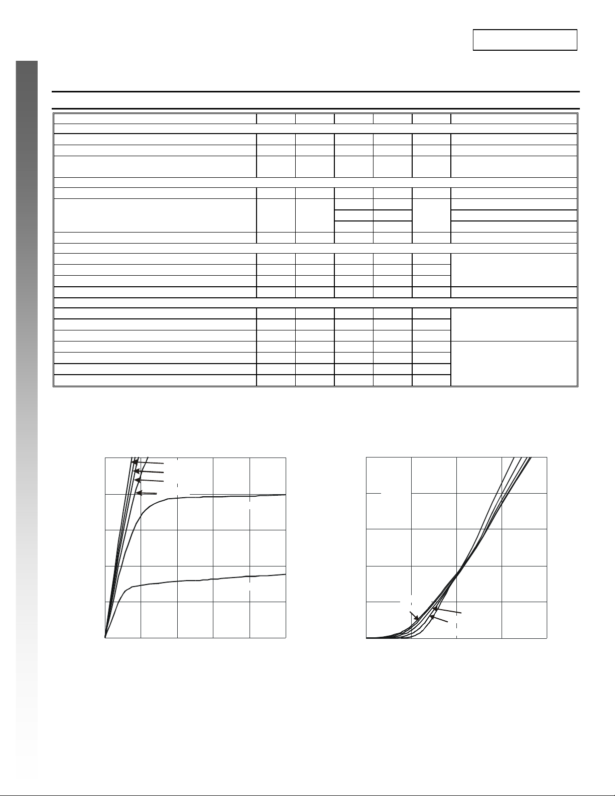
(A)
EN
20
16
12
V = 4.5V
GS
V = 3.5V
GS
V = 3.0V
GS
V = 2.5V
GS
V = 2.0V
DMG3415UFY4
-16
BV
DSS
⎯ ⎯
DSS
I
⎯ ⎯
GSS
V
GS(th
-0.3 -0.55 -1.0 V
⎯ ⎯
-1.0
±10
±500
31 39
R
DS (ON)
⎯
40 52
51 65
|Y
| ⎯
fs
C
iss
C
oss
C
rss
R
Q
Q
s
Q
d
t
D(on
t
t
D(off
t
f
⎯
⎯
⎯
⎯
⎯
⎯
⎯
⎯
⎯
⎯
⎯
7.9
281.9
152.0
37.9
250
10
1.5
2.4
79.0
175.2
884.5
568
⎯
⎯
⎯
⎯
⎯
⎯
⎯
⎯
⎯
⎯
⎯
⎯
20
V = 5V
16
GS
DS
(A)
12
V
VGS = 0V, ID = -250μA
μA
VDS = -16V, VGS = 0V
V
μA
nA
= ±8V, VDS = 0V
GS
V
= ±5V, VDS = 0V
GS
VDS = VGS, ID = -250μA
V
= -4.5V, ID = -4.0A
mΩ
pF
pF
pF
GS
V
= -2.5V, ID = -3.5A
GS
V
= -1.8V, ID = -2.0A
GS
S
VDS = -5V, ID = -2.5A
V
= -10V, VGS = 0V
DS
f = 1.0MHz
Ω
VDS = 0V, V
nC
nC
= -4.5V, V
V
GS
nC
ns
ns
V
= -10V, V
ns
DS
R
= 2.5Ω, RG = 3.0Ω
D
ns
= 0V, f = 1.0MHz
GS
= -10V, ID = -4A
DS
= -4.5V,
GS
8
D
I, D
V = 1.5V
GS
4
0
01 2345
V , DRAIN-SOURCE VOLTAGE (V)
DS
Fig. 1 Typical Output Ch ar acteristic
DMG3415UFY4
Document number: DS31842 Rev. 4 - 2
2 of 6
www.diodes.com
8
AI
D
I, D
4
0
T = 150°C
A
T = 125°C
A
T = 25°C
T = -55°C
A
T = 85°C
A
A
0.5 1 1.5 2 2.5
V , GATE-SOURCE VOLTAGE (V)
GS
Fig. 2 Typical Transfer Characteristic
December 2009
© Diodes Incorporated
AIN
 Loading...