Diodes DMG1026UV User Manual

DMG1026UV
Product Summary
I
V
R
(BR)DSS
60V
1.8 @ V
2.1 @ VGS = 4.5V
DS(ON)
GS
= 10V
D
TA = +25°C
440mA
410mA
Description
This new generation MOSFET has been designed to minimize the on-
state resistance (R
performance, making it ideal for high efficiency power management
applications.
) and yet maintain superior switching
DS(ON)
Applications
• Battery Operated Systems and Solid-State Relays
• Drivers: Relays, Solenoids, Lamps, Hammers, Displays,
Memories, Transistors, etc.
• DC-DC Converters
• Power Management Functions
ESD PROTECTED TO 2kV
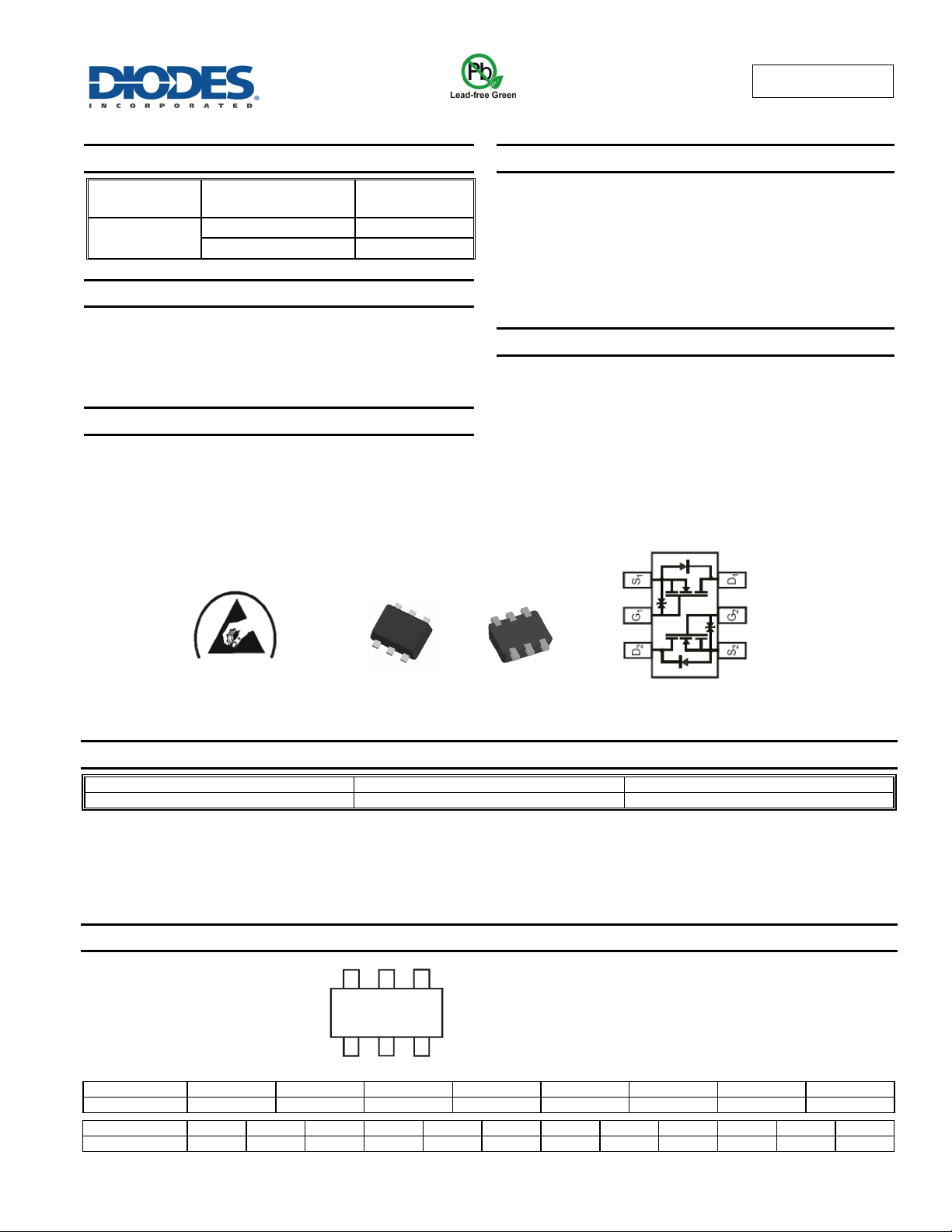
Top View
SOT563
DUAL N-CHANNEL ENHANCEMENT MODE MOSFET
Features
• Low On-Resistance
• Low Input Capacitance
• Fast Switching Speed
• Low Input/Output Leakage
• Totally Lead-Free & Fully RoHS Compliant (Notes 1 & 2)
• Halogen and Antimony Free. “Green” Device (Note 3)
• Qualified to AEC-Q101 Standards for High Reliability
Mechanical Data
• Case: SOT563
• Case Material: Molded Plastic, “Green” Molding Compound. UL
Flammability Classification Rating 94V-0
• Moisture Sensitivity: Level 1 per J-STD-020
• Terminal Connections: See Diagram Below
• Weight: 0.006 grams (approximate)
Bottom View
Top View
Pin Definition/Schematic
Ordering Information (Note 4)
Part Number Case Packaging
DMG1026UV-7 SOT563 3000 / Tape & Reel
Notes: 1. No purposely added lead. Fully EU Directive 2002/95/EC (RoHS) & 2011/65/EU (RoHS 2) compliant.
2. See http://www.diodes.com/quality/lead_free.html for more information about Diodes Incorporated’s definitions of Halogen- and Antimony-free, "Green"
and Lead-free.
3. Halogen- and Antimony-free "Green” products are defined as those which contain <900ppm bromine, <900ppm chlorine (<1500ppm total Br + Cl) and
<1000ppm antimony compounds.
4. For packaging details, go to our website at http://www.diodes.com/products/packages.html.
Marking Information
Date Code Key
Year 2009 2010 2011 2012 2013 2014 2015 2016
Code W X Y Z A B C D
Month Jan Feb Mar Apr May Jun Jul Aug Sep Oct Nov Dec
Code 1 2 3 4 5 6 7 8 9 O N D
UA1
YM
DMG1026UV
Document number: DS35068 Rev. 6 - 2
UA1 = Product Type Marking Code
YM = Date Code Marking
Y = Year (ex: X = 2010)
M = Month (ex: 9 = September)
1 of 6
www.diodes.com
February 2014
© Diodes Incorporated

V
DMG1026UV
Maximum Ratings (@T
= +25°C, unless otherwise specified.)
A
Characteristic Symbol
Drain-Source Voltage
Gate-Source Voltage
= +25°C
Continuous Drain Current (Note 5) VGS = 10V
Continuous Drain Current (Note 6) VGS = 10V
Continuous Drain Current (Note 5) VGS = 4.5V
Continuous Drain Current (Note 6) VGS = 4.5V
Steady
State
t ≤ 10s
Steady
State
t ≤ 10s
T
A
= +85°C
T
A
= +25°C
T
A
= +85°C
T
A
= +25°C
T
A
= +85°C
T
A
T
= +25°C
A
= +85°C
T
A
Pulsed Drain Current (Note 7)
Thermal Characteristics
Characteristic Symbol Max Unit
Power Dissipation (Note 5)
Thermal Resistance, Junction to Ambient @TA = 25°C (Note 5) R
Power Dissipation (Note 6) t ≤ 10s
Thermal Resistance, Junction to Ambient @TA = 25°C (Note 6) t ≤ 10s R
Operating and Storage Temperature Range
alue Unit
V
DSS
V
GSS
I
D
I
D
I
D
I
D
I
DM
P
D
JA
P
D
JA
T
, T
J
STG
60 V
±20 V
410
300
440
320
380
270
410
295
mA
mA
mA
mA
1.0 A
0.58 W
213 °C/W
0.65 W
192 °C/W
-55 to +150 °C
Electrical Characteristics (@T
= +25°C, unless otherwise specified.)
A
Characteristic Symbol Min Typ Max Unit Test Condition
OFF CHARACTERISTICS (Note 8)
Drain-Source Breakdown Voltage
Zero Gate Voltage Drain Current TJ = +25°C I
Gate-Source Leakage
BV
I
DSS
DSS
GSS
60
— —
— —
— —
—
— V
1.0 µA
±50 nA
±150 nA
VGS = 0V, ID = 250A
VDS = 50V, VGS = 0V
= ±5V, VDS = 0V
V
GS
= ±10V, VDS = 0V
V
GS
ON CHARACTERISTICS (Note 8)
Gate Threshold Voltage
Static Drain-Source On-Resistance
Forward Transfer Admittance
Continuous Source Current (Note 8)
Diode Forward Voltage
V
GS(th)
R
DS (ON)
|Y
V
fs
I
S
SD
0.5 — 1.8 V
—
—
80 580 — mS
|
— —
— 0.8 1.3 V
1.2 1.8
1.4 2.1
200 mA -
VDS = VGS, ID = 250A
= 10V, ID = 500mA
V
GS
V
= 4.5V, ID = 200mA
GS
VDS = 10V, ID = 200mA
VGS = 0V, IS = 200mA
DYNAMIC CHARACTERISTICS (Note 9)
Input Capacitance
Output Capacitance
Reverse Transfer Capacitance
Gate Resistance
Total Gate Charge
Gate-Source Charge
Gate-Drain Charge
Turn-On Delay Time
Turn-On Rise Time
Turn-Off Delay Time
Turn-Off Fall Time
Notes: 5. Device mounted on FR-4 PCB with minimum recommended pad layout, single sided.
6. Device mounted on FR-4 PCB with minimum recommended pad layout, measured in t 10s.
7. Repetitive rating, pulse width limited by junction temperature, 10µs pulse, duty cycle = 1%
8. Short duration pulse test used to minimize self-heating effect.
9. Guaranteed by design. Not subject to production testing.
C
C
C
R
Q
Q
Q
t
D(on)
t
D(off)
iss
oss
rss
gd
t
t
g
g
gs
r
f
DMG1026UV
Document number: DS35068 Rev. 6 - 2
—
—
—
—
—
—
—
—
—
—
—
2 of 6
www.diodes.com
32
4.4
2.9
126
0.45
0.08
0.08
3.4
3.4
26.4
16.3
—
—
—
—
—
—
—
—
—
—
—
= 25V, VGS = 0V,
V
pF
pC
ns
ns
ns
ns
DS
f = 1.0MHz
VDS = 0V, VGS = 0V, f = 1MHz
= 4.5V, VDS = 10V,
V
GS
= 250mA
I
D
= 10V, VDS = 30V,
V
GS
= 150, RG = 25,
R
L
= 200mA
I
D
February 2014
© Diodes Incorporated
 Loading...