

Page 1
θ
Features
• 5-line ESD Protection
• Sub-miniature Package (1.6 x 1.6mm)
• Low Capacitance – 42pF typ @ V
• Provides a High Level of Protection from ESD to IEC61000-4-2
• ±30kV Contact Discharge
• ±30kV Air Discharge
• Lead Free/RoHS Compliant (Note 1)
• "Green" Device (Note 2)
• Qualified to AEC-Q101 Standards for High Reliability
NEW PRODUCT
= 0V
R
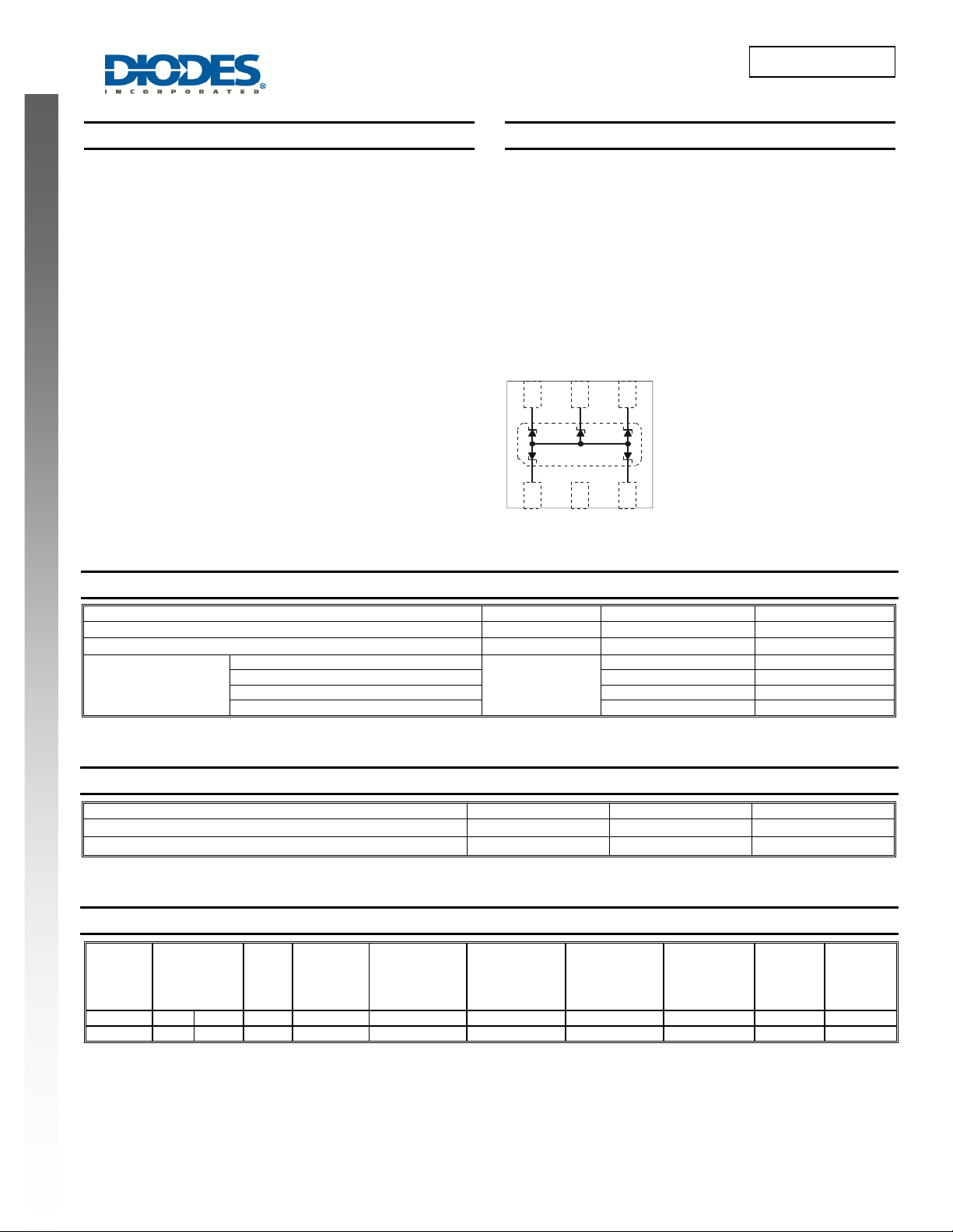
BOTTOM VIEW
DMF05LCFLP
FIVE ELEMENT COMMON ANODE ESD-PROTECTION DIODE ARRAY
Mechanical Data
• Case: DFN1616-6
• Case Material: Molded Plastic, “Green” Molding Compound.
UL Flammability Classification Rating 94V-0
• Moisture Sensitivity: Level 1 per J-STD-020
• Terminals: Solderable per MIL-STD-202, Method 208
• Lead Free Plating (NiPdAu Finish over Copper leadframe).
• Polarity: Pin 1 Dot and Center Pad Notch, See Diagram
• Marking Information: See Page 2
• Ordering Information: See Page 2
• Weight: 0.004 grams (approximate)
DFN1616-6
654
123
TOP VIEW
Internal Schematic
Maximum Ratings @T
= 25°C unless otherwise specified
A
Characteristic Symbol Value Unit
Peak Pulse Current, 8/20μs waveform, single shot, per IEC61000-4-5
Peak Pulse Power, 8/20μs waveform, single shot, per IEC61000-4-5
Human Body Model
ESD Rating
Machine Model 400 V
IEC61000-4-2 Air Discharge 30 kV
I
PPM
P
PP
ESD
5 A
70 W
8 kV
IEC61000-4-2 Contact Discharge 30 kV
Thermal Characteristics
Characteristic Symbol Value Unit
Thermal Resistance Junction to Ambient Air (Note 3)
Operating and Storage Temperature Range
R
JA
, T
T
J
STG
Electrical Characteristics @T
Reverse
Standoff
Voltage
V
RWM
= 1μA
I
RWM
Min (V) Min (V) Max (V)
@
Breakdown
Voltage
@ IT
V
BR
Current
Max. Reverse
Test
(mA) IR (μA) V
I
T
= 25°C unless otherwise specified
A
Leakage @
V
RWM
(Note 4)
Max. Clamping
@ I
per IEC61000-4-5
Voltage
= 1A
PP
(V) V
C
Max. Clamping
Voltage V
= 5A
@ I
PP
per IEC61000-4-5
(V) VF (V) VF (V) C
C
Max. Forward
c
per IEC61000-4-5
Clamping
Voltage V
= 1A
@ I
F
5.0 6 8 1.0 0.1 9.5 12.5 2 4 50 25
Notes: 1. No Purposefully added Lead.
2. Diodes Inc.'s "Green" policy can be found on our website at http://www.diodes.com/products/lead_free/index.php.
DMF05LCFLP
Document number: DS32004 Rev. 3 - 2
3. Part mounted on FR-4 PC board with recommended pad layout, which can be found on our website at http://www.diodes.com/datasheets/ap02001.pdf.
Only one switching diode powered on.
4. Short duration pulse test used to minimize self-heating effect.
1 of 4
www.diodes.com
256
-55 to +150
Max. Forward
Clamping
Voltage V
F
@ I
per IEC61000-4-5
= 5A
F
F
°C/W
Max Total
Capacitance
= 0V
V
R
f = 1MHz
(pF) CT(pF)
T
© Diodes Incorporated
°C
Typical Total
Capacitance
VR = 2.5V
f = 1MHz
July 2010
Page 2
TANT
O
U
O
R
RD C
URRENT
NSTAN
TANEO
US R
R
OLTAG
C, TOT
CAPACITAN
C
A
NEW PRODUCT
DMF05LCFLP
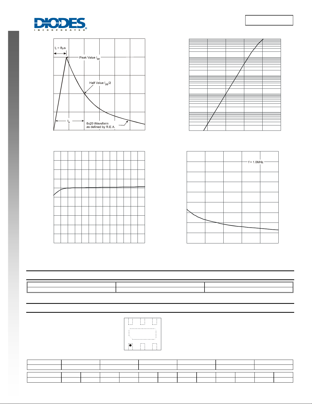
100
(mA)
100
PppP
I , PEAK PULSE CURRENT (%I )
E (V)
SE V
EVE
50
10
0
0
8
6
4
20 40
t, TIME ( s)
Fig. 1 Pulse Waveform
μ
60
10
1
WA
S F
0.1
ANE
0.01
F
0.001
I , INS
0.5 0.6 0.7 0.8 0.9 1.0
V , INSTANTANEOUS FORWARD VOLTAGE (V)
F
Fig. 2 Typical Forward Characteristics
100
90
80
E (pF)
70
60
50
AL
40
T
2
R
V, I
0
0.5 1.5 2.5 3.5 4.5 5.5 6.5
I , INSTANTANEOUS REVERSE CURRENT (nA)
R
Fig. 3 Typical Reverse Characteristics
30
20
10
012345
Fig. 4 Typical Capacit ance vs. Reverse Voltage
V , REVERSE VOLTAGE (V)
R
Ordering Information (Note 5)
Part Number Case Packaging
DMF05LCFLP-7 DFN1616-6 3000/Tape & Reel
Notes: 5. For packaging details, go to our website at http://www.diodes.com/datasheets/ap02007.pdf.
Marking Information
A10 YM
Date Code Key
Year 2010 2011 2012 2013 2014 2015
Code X Y Z A B C
Month Jan Feb Mar Apr May Jun Jul Aug Sep Oct Nov Dec
Code 1 2 3 4 5 6 7 8 9 O N D
10 = Product Type Marking Code
YM = Date Code Marking
Y = Year (ex: X = 2010)
M = Month (ex: 9 = September)
DMF05LCFLP
Document number: DS32004 Rev. 3 - 2
2 of 4
www.diodes.com
July 2010
© Diodes Incorporated
Page 3

Package Outline Dimensions
NEW PRODUCT
Suggested Pad Layout
DMF05LCFLP
A
A1
D
e
E
E2
b
D2
Y
X2
C
Z
A3
L
G
X1
Dimensions Value (in mm)
DFN1616-6
Dim Min Max Typ
A 0.545 0.605 0.575
A1 0 0.05 0.02
A3
⎯ ⎯
b 0.20 0.30 0.25
D 1.55 1.675 1.60
D2 1.10 1.30 1.20
E 1.55 1.675 1.60
e
⎯ ⎯
E2 0.30 0.50 0.40
L 0.275 0.375 0.325
All Dimensions in mm
Z 1.3
G 0.175
X1 0.50
X2 0.525
Y 0.30
C 0.50
0.13
0.50
DMF05LCFLP
Document number: DS32004 Rev. 3 - 2
3 of 4
www.diodes.com
July 2010
© Diodes Incorporated
Page 4

DIODES INCORPORATED MAKES NO WARRANTY OF ANY KIND, EXPRESS OR IMPLIED, WITH REGARDS TO THIS DOCUMENT,
INCLUDING, BUT NOT LIMITED TO, THE IMPLIED WARRANTIES OF MERCHANTABILITY AND FITNESS FOR A PARTICULAR PURPOSE
(AND THEIR EQUIVALENTS UNDER THE LAWS OF ANY JURISDICTION).
Diodes Incorporated and its subsidiaries reserve the right to make modifications, enhancements, improvements, corrections or other changes
without further notice to this document and any product described herein. Diodes Incorporated does not assume any liability arising out of the
application or use of this document or any product described herein; neither does Diodes Incorporated convey any license under its patent or
trademark rights, nor the rights of others. Any Customer or user of this document or products described herein in such applications shall assume
all risks of such use and will agree to hold Diodes Incorporated and all the companies whose products are represented on Diodes Incorporated
website, harmless against all damages.
Diodes Incorporated does not warrant or accept any liability whatsoever in respect of any products purchased through unauthorized sales channel.
Should Customers purchase or use Diodes Incorporated products for any unintended or unauthorize d application, Customers shall indemnify and
hold Diodes Incorporated and its representatives harmless against all claims, damages, expenses, and attorney fees arising out of, directly or
indirectly, any claim of personal injury or death associated with such unintended or unauthorized application.
Products described herein may be covered by one or more United States, international or foreign patents pending. Product names and markings
noted herein may also be covered by one or more United States, international or foreign trademarks.
NEW PRODUCT
Diodes Incorporated products are specifically not authorized for use as critical components in life support devices or systems without the express
written approval of the Chief Executive Officer of Diodes Incorporated. As used herein:
A. Life support devices or systems are devices or systems which:
1. are intended to implant into the body, or
labeling can be reasonably expected to result in significant injury to the user.
B. A critical component is any component in a life support device or system whose failure to perform can be reasonably expected to cause the
failure of the life support device or to affect its safety or effectiveness.
Customers represent that they have all necessary expertise in the safety and regulatory ramifications of their life support devices or systems, and
acknowledge and agree that they are solely responsible for all legal, regulatory and safety-related requirements concerning their products and any
use of Diodes Incorporated products in such safety-critical, life support devices or systems, notwithstanding any devices- or systems-related
information or support that may be provided by Diodes Incorporated. Further, Customers must fully indemnify Diodes Incorporated and its
representatives against any damages arising out of the use of Diodes Incorporated products in such safety-critical, life support devices or systems.
Copyright © 2010, Diodes Incorporated
www.diodes.com
2. support or sustain life and whose failure to perform when properly used in accordance with instructions for use provided in the
IMPORTANT NOTICE
LIFE SUPPORT
DMF05LCFLP
DMF05LCFLP
Document number: DS32004 Rev. 3 - 2
4 of 4
www.diodes.com
July 2010
© Diodes Incorporated
 Loading...