

Page 1
A
f
1
40V COMPLEMENTARY PAIR ENHANCEMENT MODE MOSFET
Product Summary
I
max
Device
Q1 40V
Q2 -40V
V
(BR)DSS
R
DS(on)
45mΩ @ V
60mΩ @ VGS= 4.5V
45mΩ @ V
60mΩ @ VGS= -4.5V
max
GS
= -10V
GS
= 10V
D
TA = 25°C
(Notes 3 & 5)
5.5A
4.2A
-5.8A
-4.2A
Description and Applications
This MOSFET has been designed to ensure that R
channel FET are matched to minimize losses in both arms of the
bridge. The DMC4040SSD is optimized for use in 3 phases brushless
DC motor circuits (BLDC), CCFL backlighting.
• 3 phases BLDC motor
• CCFL backlighting
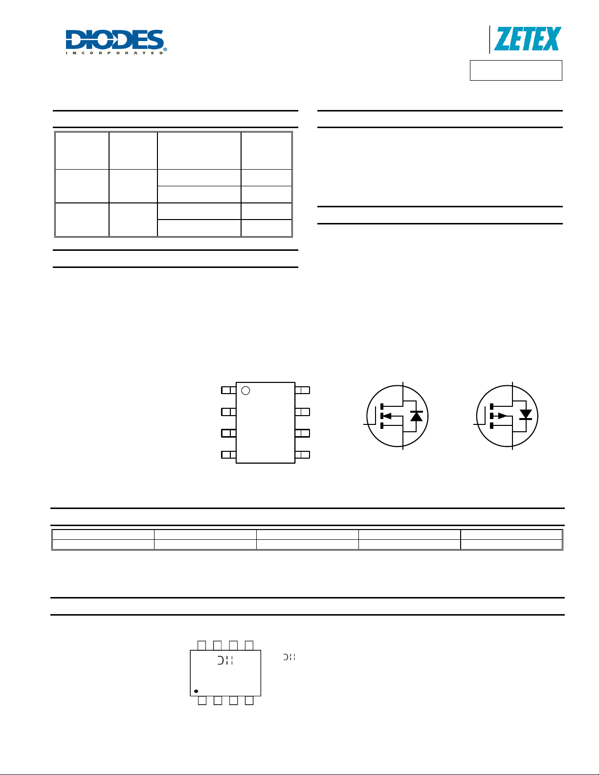
SO-8
G1
S2
G2
Top View
DS(on)
of N and P
Top View
Product Line o
Diodes Incorporated
DMC4050SSD
Features and Benefits
• Matched N & P R
• Fast switching – Minimizes switching losses
• Dual device – Reduces PCB area
• "Green" component and RoHS compliant (Note 1)
• Qualified to AEC-Q101 Standards for High Reliability
- Minimizes power losses
DS(on)
Mechanical Data
• Case: SO-8
• Case Material: Molded Plastic, “Green” Molding Compound. UL
Flammability Classification Rating 94V-0 (Note 1)
• Moisture Sensitivity: Level 1 per J-STD-020
• Terminals: Finish - Matte Tin annealed over Copper lead frame.
Solderable per MIL-STD-202, Method 208
• Weight: 0.074 grams (approximate)
D1S1
D1
D2
D2
G1
D
G2
S1
Equivalent Circuit
D2
S2
Ordering Information (Note 1)
Product Marking Reel size (inches) Tape width (mm) Quantity per reel
DMC4050SSD-13 C4050SD 13 12 2,500
Notes: 1. Diodes, Inc. defines “Green” products as those which are RoHS compliant and contain no halogens or antimony compounds; further information about
Diodes Inc.’s “Green” Policy can be found on our website. For packaging details, go to our website.
Marking Information
DMC4050SSD
Document number: DS33310 Rev. 2 - 2
C4050SD
YY
WW
= Manufacturer’s Marking
C4050SD = Product Type Marking Code
YYWW = Date Code Marking
YY = Year (ex: 10 = 2010)
WW = Week (01 - 53)
1 of 11
www.diodes.com
March 2011
© Diodes Incorporated
Page 2
A
f
Product Line o
Diodes Incorporated
DMC4050SSD
Maximum Ratings @T
Drain-Source Voltage
Gate-Source Voltage
Continuous Drain Current
Pulsed Drain Current
Continuous Source Current (Body diode) (Notes 3 & 5)
Pulsed Source Current (Body diode) (Notes 4 & 5)
Thermal Characteristics @T
Power Dissipation
Linear Derating Factor
Thermal Resistance, Junction to Ambient
Thermal Resistance, Junction to Lead (Notes 5 & 7)
Operating and Storage Temperature Range
Notes: 2. For a device surface mounted on 25mm x 25mm x 1.6mm FR4 PCB with high coverage of single sided 1oz copper, in still air conditions; the device is
measured when operating in a steady-state condition.
DMC4050SSD
Document number: DS33310 Rev. 2 - 2
3. Same as note (2), except the device is measured at t ≤ 10 sec.
4. Same as note (2), except the device is pulsed with D = 0.02 and pulse width 300µs.
5. For a dual device with one active die.
6. For a device with two active die running at equal power.
7. Thermal resistance from junction to solder-point (at the end of the drain lead).
= 25°C unless otherwise specified
A
Characteristic Symbol N-Channel - Q1 P-Channel - Q2
V
DSS
V
(Notes 3 & 5)
= 10V
V
GS
V
= 10V
GS
Characteristic Symbol N-Channel - Q1 P-Channel - Q2 Unit
TA = 70°C (Notes 3 & 5)
(Notes 2 & 5) 4.2 -4.2
(Notes 2 & 6) 5.3 -5.3
(Notes 4 & 5)
= 25°C unless otherwise specified
A
(Notes 2 & 5)
(Notes 2 & 6)
(Notes 3 & 5)
(Notes 2 & 5)
(Notes 2 & 6) 70
(Notes 3 & 5) 58
GSS
IDM
I
SM
P
R
R
T
J, TSTG
ID
I
S
θJA
θJL
D
40 -40
±20 ±20
5.8 -5.8
4.38 -4.52
24.1 -24.9
2.5 -2.5
24.1 -24.9
1.25
10
1.8
14.3
2.14
17.2
100
51
-55 to +150 °C
Units
V
A
W
mW/°C
°C/W
2 of 11
www.diodes.com
March 2011
© Diodes Incorporated
Page 3
A
f
Thermal Characteristics
Product Line o
Diodes Incorporated
DMC4050SSD
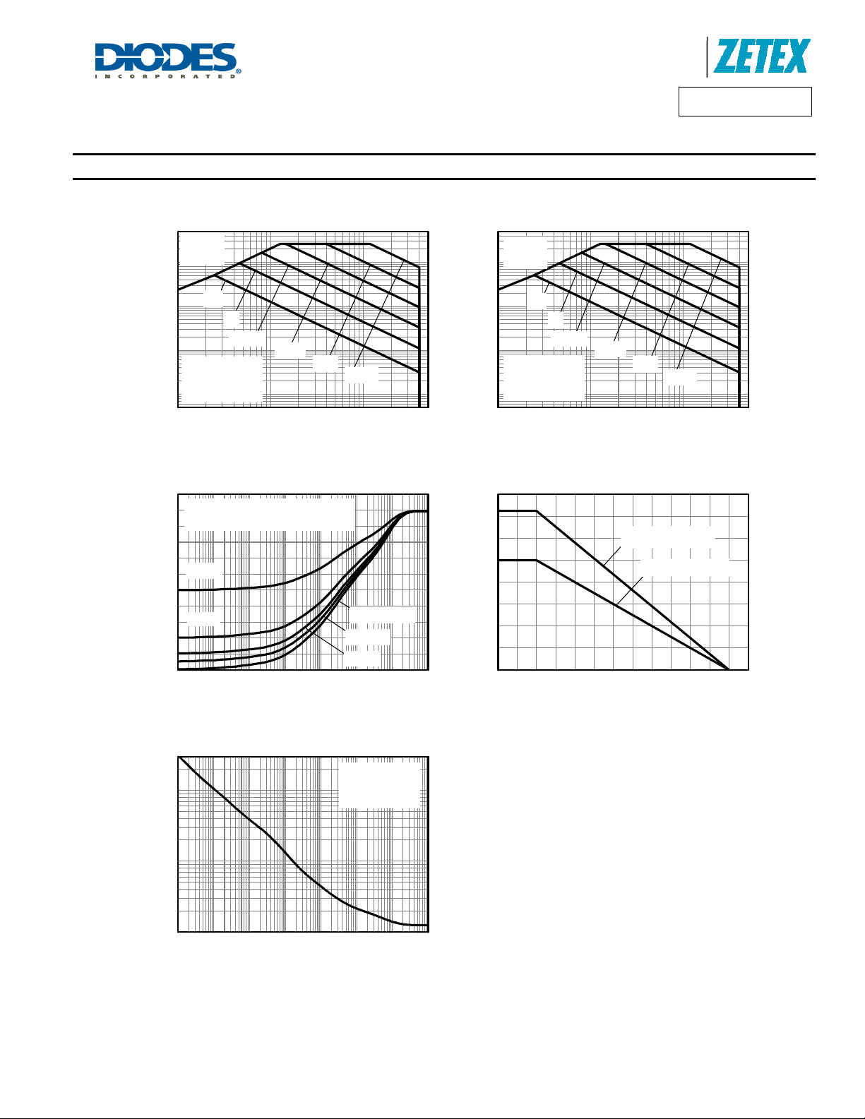
R
DS(ON)
Limited
10
DC
1
100m
Drain Current (A)
D
10m
I
0.1 1 10
1s
100ms
Single Pulse
T
= 25°C
amb
One active die
10ms
1ms
100us
VDS Drain-Source Voltage (V)
N-channe l Safe O p erating A rea
R(theta junction-to-ambient), R
100
One active die
80
D=0.5
60
40
D=0.2
20
Thermal Resistance (°C/W)
0
100µ 1m 10m 100m 1 10 100 1k
Pulse Width (s)
θJA
Single Pulse
D=0.05
D=0.1
R
DS(ON)
Limited
10
DC
1
1s
amb
100ms
= 25°C
100m
Drain Current (A)
-I
Single Pulse
T
D
10m
One active die
0.1 1 10
10ms
1ms
100us
-VDS Drain-Source Voltage (V)
P-channel Safe Operating Area
2.0
1.5
1.0
0.5
0.0
0 25 50 75 100 125 150
Max Power Dissipation (W)
Temperature (°C)
Two active die
One active die
Transient Thermal Impedance
Single Pulse
T
= 25°C
100
10
amb
One active die
Derating Curve
Maximum Power (W)
1
100µ 1m 10m 100m 1 10 100 1k
Pulse Width (s)
Pulse Power Dissipation
DMC4050SSD
Document number: DS33310 Rev. 2 - 2
3 of 11
www.diodes.com
© Diodes Incorporated
March 2011
Page 4
A
f
)
g
g
g
g
r
R
C
U
R
R
T
RAIN
CUR
R
N
T
Electrical Characteristics N-CHANNEL @T
Characteristic Symbol Min Typ Max Unit Test Condition
OFF CHARACTERISTICS (Note 8)
Drain-Source Breakdown Voltage
Zero Gate Voltage Drain Current TJ = 25°C I
Gate-Source Leakage
ON CHARACTERISTICS (Note 8)
Gate Threshold Voltage
Static Drain-Source On-Resistance
Forward Transfer Admittance
Diode Forward Voltage (Note 8)
DYNAMIC CHARACTERISTICS (Note 9)
Input Capacitance
Output Capacitance
Reverse Transfer Capacitance
Gate Resistance
Total Gate Charge
Gate-Source Charge
Gate-Drain Charge
Turn-On Delay Time
Turn-On Rise Time
Turn-Off Delay Time
Turn-Off Fall Time
Notes: 8. Short duration pulse test used to minimize self-heating effect.
9. Guaranteed by design. Not subject to production testing.
30
= 25°C unless otherwise specified
A
40 - - V
BV
DSS
- - 1.0
DSS
- - ±100 nA
I
GSS
0.8 1.3 1.8 V
V
GS(th
R
DS (ON)
|Y
V
SD
-
|
fs
- 12.6 - S
- 0.7 1.0 V
20
33
C
C
C
R
Q
Q
Q
t
D(on)
t
D(off)
iss
oss
rss
t
t
s
d
f
- 1790.8 -
- 160.6 -
- 120.5 -
- 1.03 -
- 37.56 -
- 7.8 -
- 6.6 -
8.08
-
15.14
-
24.29
-
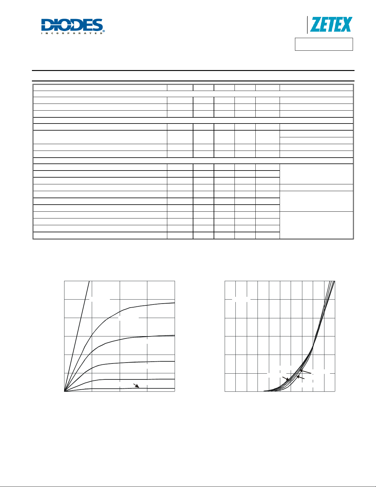
5.27
-
30
25
V = 8.0V
GS
25
V = 5V
DS
(A)
EN
20
V = 4.5V
GS
(A)
20
E
15
V = 4.0V
GS
AIN
10
D
I, D
V = 3.5V
GS
5
V = 3.0V
V = 2.5V
0
0 0.5 1 1.5 2
V , DRAIN-SOURCE VOLTAGE (V)
DS
GS
GS
Fig. 1 Typica l O ut put Chara ct er istic
DMC4050SSD
Document number: DS33310 Rev. 2 - 2
www.diodes.com
4 of 11
15
10
D
I, D
5
0
012345
Product Line o
Diodes Incorporated
DMC4050SSD
VGS = 0V, ID = 250μA
μA
VDS = 40V, VGS = 0V
VGS = ±20V, VDS = 0V
VDS = VGS, ID = 250μA
= 10V, ID = 3A
45
60
- ns
- ns
- ns
- ns
V , GATE-SOURCE VOLT AGE (V)
GS
Fig. 2 Typical Transfer Characteristic
V
mΩ
GS
VGS = 4.5V, ID = 3A
VDS = 5V, ID = 3A
VGS = 0V, IS = 1A
pF
pF
pF
Ω
nC
nC
nC
T = 125°C
A
= 20V, VGS = 0V,
V
DS
f = 1.0MHz
VDS = 0V, VGS = 0V, f = 1MHz
V
= 10V, VDS = 20V,
GS
I
= 3A
D
V
= 10V, VDS = 20V,
GS
= 3A
I
D
T = 150°C
A
T = 25°C
A
T = -55°C
A
T = 85°C
A
March 2011
© Diodes Incorporated
Page 5

A
f
R
RAIN-SOUR
CE O
N-R
TAN
C
OUR
CE C
U
R
R
T
Ω
0.06
0.05
0.04
Ω
E ( )
V = 10V
GS
0.03
0.04
ESIS
Product Line o
Diodes Incorporated
DMC4050SSD
V = 4.5V
GS
0.03
0.02
V = 10V
GS
0.01
DS(ON)
R , DRAIN-SOURCE ON-RESISTANCE ( )
0
0 5 10 15 20 25 30
I , DRAIN-SOURCE CURRENT (A)
D
Fig. 3 Typical On-Resistance
vs. Drain C urrent and G ate V oltage
1.7
V = 10V
1.5
GS
I = 20A
D
1.3
1.1
0.9
DSON
R , DRAIN -SOURCE
0.7
ON-RESISTANCE (NORMALIZED)
0.5
-50 -25 0 25 50 75 100 125 150
T , AMBIENT TEMPERATURE (°C)
A
Fig. 5 On- Resistance Variation with Temperature
3.0
2.7
V = 4.5V
GS
I = 10A
D
T = 150°C
A
0.02
0.01
, D
DS(ON)
0
0 5 10 15 20 25 30
I , DRAIN CURRENT (A)
D
T = 125°C
A
T = 85°C
A
T = 25°C
A
T = -55°C
A
Fig. 4 Typical On-Resistance
vs. Drain C urrent and Temperatu r e
0.06
Ω
0.05
0.04
0.03
V = 4.5V
GS
I = 10A
D
0.02
V = 10V
0.01
DSON
R , DRAIN-SOURCE ON-RESISTANCE ( )
0
-50 -25 0 25 50 75 100 125 150
T , AMBIENT TEMPERATURE (°C)
A
Fig. 6 On- Resistance Variation with Temperature
GS
I = 20A
D
20
18
2.4
2.1
1.8
I = 1mA
1.5
D
1.2
I = 250µA
0.9
D
0.6
GS(TH)
0.3
V , GATE THRESHOLD VOLTAGE (V)
0
-50 -25 0 25 50 75 100 125 150
T , AMBIENT TEMPERATURE (°C)
A
Fig. 7 Gate Threshold Variation vs. Ambient Temperature
DMC4050SSD
Document number: DS33310 Rev. 2 - 2
5 of 11
www.diodes.com
16
(A)
14
EN
12
T = 25°C
A
10
8
6
S
I, S
4
2
0
0.2 0.4 0.6 0.8 1.0 1.2
V , SOURCE-DRAIN VOLT AGE (V)
SD
Fig. 8 Diode Forward Vol tage vs. Current
March 2011
© Diodes Incorporated
Page 6

A
f
C, C
P
C
T
C
F
GE CUR
R
T
GAT
OUR
C
OLTAG
T
R
T T
H
R
R
TANC
10,000
)
1,000
E (p
AN
I
A
A
100
10
0 5 10 15 20 25 30
V , DRAIN-SOURCE VOLTAGE (V)
DS
C
iss
C
oss
C
rss
Fig. 9 Typical Total Capacitance
f = 1MHz
10,000
(nA)
1,000
EN
100
10
DSS
I , LEAKA
1
0 5 10 15 20 25 30 35 40
Product Line o
Diodes Incorporated
DMC4050SSD
T = 150°C
A
T = 125°C
A
T = 85°C
A
T = 25°C
A
V , DRAIN-SOURCE VOLTAGE (V)
DS
Fig. 10 Typical Leakage Current
vs. Drain-S ource Voltage
10
V = 20V
8
E (V)
6
E V
4
E-S
2
GS
V,
0
0 5 10 15 20 25 30 35 40
Q , TOTAL GATE CHARGE (nC)
g
DS
I = 12A
D
Fig. 11 Gate-Ch ar g e C haracte r i s t ics
1
E
D = 0.7
D = 0.5
D = 0.3
ESIS
0.1
D = 0.1
MAL
E
0.01
ANSIEN
r(t),
0.001
D = 0.05
D = 0.02
D = 0.01
D = 0.005
D = Single Pulse
0.0001
0.001 0.01 0.1 1 10 100 1,000
t , PULSE DURATION TIME (s)
1
D = 0.9
R (t) = r(t) *
θ
JA
R = 94°C/W
JA
P(pk)
t
1
t
2
T - T = P * R (t)
JA JA12θ
Duty Cycle, D = t /t
R
θθJA
Fig. 12 Transi ent Thermal Response
DMC4050SSD
Document number: DS33310 Rev. 2 - 2
6 of 11
www.diodes.com
March 2011
© Diodes Incorporated
Page 7

A
f
)
g
g
g
g
)
r
)
R
CUR
RENT
R
CUR
RENT
Product Line o
Diodes Incorporated
DMC4050SSD
Electrical Characteristics P-CHANNEL
Characteristic Symbol Min Typ Max Unit Test Condition
OFF CHARACTERISTICS (Note 8)
Drain-Source Breakdown Voltage
Zero Gate Voltage Drain Current TJ = 25°C I
Gate-Source Leakage
ON CHARACTERISTICS (Note 8)
Gate Threshold Voltage
Static Drain-Source On-Resistance
Forward Transfer Admittance
Diode Forward Voltage (Note 8)
DYNAMIC CHARACTERISTICS (Note 9)
Input Capacitance
Output Capacitance
Reverse Transfer Capacitance
Gate Resistance
Total Gate Charge
Gate-Source Charge
Gate-Drain Charge
Turn-On Delay Time
Turn-On Rise Time
Turn-Off Delay Time
Turn-Off Fall Time
Notes: 8. Short duration pulse test used to minimize self-heating effect.
9. Guaranteed by design. Not subject to production testing.
30
= 25°C unless otherwise specified
@TA
-40 - - V
BV
DSS
- - -1.0
DSS
I
GSS
- - ±100 nA
V
GS(th
R
DS (ON)
|Y
V
fs
SD
-0.8 -1.3 -1.8 V
-
|
- 16.6 - S
- -0.7 -1.0 V
28
30
- 1643.17 - pF
- 179.13 - pF
- 127.82 - pF
- 6.43 -
- 33.66 - nC
- 5.54 - nC
- 7.30 - nC
- 6.85 - ns
- 14.72 - ns
- 53.65 - ns
- 30.86 - ns
C
C
t
t
C
oss
rss
R
Q
Q
Q
D(on
t
D(off
t
iss
s
d
f
30
45
60
VGS = 0V, ID = -250μA
μA
VDS = -40V, VGS = 0V
VGS = ±20V, VDS = 0V
VDS = VGS, ID = -250μA
= -10V, ID = -3A
V
mΩ
GS
VGS = -4.5V, ID = -3A
VDS = -5V, ID = -3A
VGS = 0V, IS = -1A
V
= -20V, VGS = 0V,
DS
f = 1.0MHz
Ω
VDS = 0V, VGS = 0V, f = 1MHz
V
= -10V, VDS = -20V,
GS
I
= -3A
D
V
= -10V, VDS = -20V,
GS
= -3A
I
D
(A)
AIN
D
-I , D
25
20
15
10
(A)
AIN
5
-I , D
25
20
V = -5V
DS
T = 85°C
A
T = 25°C
A
T = -55°C
A
T = 150°C
A
T = 125°C
A
15
10
D
5
0
0 0.5 1 1.5 2
-V , DRAIN-SOURCE VOLTAGE (V)
DS
Fig. 13 Typical Output Characteristic
DMC4050SSD
Document number: DS33310 Rev. 2 - 2
www.diodes.com
7 of 11
0
012345
-V , GATE-SOURCE VOLTAGE (V)
GS
Fig. 14 Typical Transfer Characteristic
© Diodes Incorporated
March 2011
Page 8

A
f
R
R
OUR
CE O
R
TANC
R
R
OUR
CE O
R
TANC
7
R
RAIN-SOUR
C
R
R
OUR
CE ON-R
TANC
O
U
R
CE C
U
R
R
T
0.05
Ω
E ( )
0.04
Ω
E ( )
V = -10V
GS
0.04
0.03
ESIS
N-
0.02
ESIS
N-
0.03
V = -4.5V
GS
V = -10V
GS
0.02
AIN-S
, D
0.01
AIN-S
0.01
, D
Product Line o
Diodes Incorporated
DMC4050SSD
T = 150°C
A
T = 125°C
A
T = 85°C
A
T = 25°C
A
T = -55°C
A
DS(ON)
0
0 5 10 15 20 25 30
-I , DRAIN-SOURCE CURRENT (A)
D
Fig. 15 Typical On-Resistance
vs. Drain C urrent an d G at e Vol t age
1.
1.5
E
1.3
1.1
, D
0.9
DSON
0.7
ON-RESISTA NCE (NORMA LIZED)
0.5
-50 -25 0 25 50 75 100 125 150
T , AMBIENT TEMPERATURE (°C)
A
Fig. 17 On- R esista nce V ar i ation with Temperatu r e
2.0
V = -10V
GS
I = -20A
D
V = -4.5V
GS
I = -10A
D
DS(ON)
0
0 5 10 15 20 25 30
-I , DRAIN CURRENT (A)
D
Fig. 16 Typical On-Resistance
vs. Drain C urrent and Tempera tu r e
0.06
Ω
E ( )
0.05
0.04
ESIS
0.03
0.02
AIN-S
0.01
, D
DSON
0
-50 -25 0 25 50 75 100 125 150
T , AMBIENT TEMPERATURE (°C)
A
Fig. 18 On- Resistance Variation with Temperatu r e
V = -4.5V
GS
I = -10A
D
V = -10V
GS
I = -20A
D
20
18
1.5
I = -1mA
1.0
I = -250µA
D
D
0.5
GS(TH)
-V , GATE THRESHOLD VOLTAGE (V)
0
-50 -25 0 25 50 75 100 125 150
T , AMBIENT TEMPERATURE (°C)
A
Fig. 19 Gat e Threshold Variation vs. Ambien t Temperature
(A)
EN
14
12
T = 25°C
A
10
8
6
S
-I , S
4
2
0
0.2 0.4 0.6 0.8 1.0 1.2
-V , SOURCE-DRAIN VOLT AGE (V)
SD
Fig. 20 Diode Forward Voltage vs. Current
16
DMC4050SSD
Document number: DS33310 Rev. 2 - 2
8 of 11
www.diodes.com
March 2011
© Diodes Incorporated
Page 9

A
f
C, CAPACITAN
C
F
GE CUR
R
N
T
GAT
OUR
C
OLTAG
T
RAN
N
T T
HER
R
T
N
C
10,000
)
1,000
E (p
C
iss
10,000
(nA)
1,000
E
Product Line o
Diodes Incorporated
T = 150°C
A
T = 125°C
A
DMC4050SSD
C
oss
100
10
0 5 10 15 20 25 30
-V , DRAIN-SOURCE VOLT AGE (V)
DS
C
rss
Fig. 21 Typical Total Capacitance
10
V = -20V
E (V)
E V
E-S
GS
-V ,
8
6
4
2
DS
I = -12A
D
100
T = 85°C
A
10
DSS
-I , LEAKA
T = 25°C
A
1
0 5 10 15 20 25 30 35 40
-V , DRAIN-SOURCE VOLTAGE (V)
DS
Fig. 22 Typical Leakage Current
vs. Drain-Source Voltage
0
0 5 10 15 20 25 30 35 40
Q , TOTAL GATE CHARGE (nC)
g
Fig. 23 Gate-Charge Characteristics
1
E
D = 0.7
D = 0.5
A
D = 0.3
ESIS
0.1
D = 0.1
MAL
0.01
SIE
r(t),
0.001
D = 0.05
D = 0.02
D = 0.01
D = 0.005
D = Single Pulse
0.0001
0.001 0.01 0.1 1 10 100 1,000
t , PULSE DURATION TIME (s)
D = 0.9
1
R (t) = r(t) *
θ
JA
R = 94°C/W
JA
P(pk)
t
1
t
2
T - T = P * R (t)
JA JA12θ
Duty Cycle, D = t /t
R
θθJA
Fig. 24 Transient Thermal Response
DMC4050SSD
Document number: DS33310 Rev. 2 - 2
9 of 11
www.diodes.com
March 2011
© Diodes Incorporated
Page 10

A
f
Package Outline Dimensions
E1
E
A2
A
e
b
D
Suggested Pad Layout
X
C2
Y
A3
A1
h
Detail ‘A’
°
45
C1
L
0.254
Gaug e Plan e
Seating Plane
7°~9
°
Product Line o
Diodes Incorporated
Dim Min Max
A - 1.75
A1 0.10 0.20
A2 1.30 1.50
A3 0.15 0.25
b 0.3 0.5
D 4.85 4.95
E 5.90 6.10
E1 3.85 3.95
e 1.27 Typ
h - 0.35
Detail ‘A’
Dimensions Value (in mm)
X 0.60
Y 1.55
C1 5.4
C2 1.27
L 0.62 0.82
θ
All Dimensions in mm
DMC4050SSD
SO-8
0° 8°
DMC4050SSD
Document number: DS33310 Rev. 2 - 2
10 of 11
www.diodes.com
March 2011
© Diodes Incorporated
Page 11

A
f
IMPORTANT NOTICE
DIODES INCORPORATED MAKES NO WARRANTY OF ANY KIND, EXPRESS OR IMPLIED, WITH REGARDS TO THIS DOCUMENT,
INCLUDING, BUT NOT LIMITED TO, THE IMPLIED WARRANTIES OF MERCHANTABILITY AND FITNESS FOR A PARTICULAR PURPOSE
(AND THEIR EQUIVALENTS UNDER THE LAWS OF ANY JURISDICTION).
Diodes Incorporated and its subsidiaries reserve the right to make modifications, enhancements, improvements, corrections or other changes
without further notice to this document and any product described herein. Diodes Incorporated does not assume any liability arising out of the
application or use of this document or any product described herein; neither does Diodes Incorporated convey any license under its patent or
trademark rights, nor the rights of others. Any Customer or user of this document or products described herein in such applications shall assume
all risks of such use and will agree to hold Diodes Incorporated and all the companies whose products are represented on Diodes Incorporated
website, harmless against all damages.
Diodes Incorporated does not warrant or accept any liability whatsoever in respect of any products purchased through unauthorized sales channel.
Should Customers purchase or use Diodes Incorporated products for any unintended or unauthorize d application, Customers shall indemnify and
hold Diodes Incorporated and its representatives harmless against all claims, damages, expenses, and attorney fees arising out of, directly or
indirectly, any claim of personal injury or death associated with such unintended or unauthorized application.
Products described herein may be covered by one or more United States, international or foreign patents pending. Product names and markings
noted herein may also be covered by one or more United States, international or foreign trademarks.
LIFE SUPPORT
Diodes Incorporated products are specifically not authorized for use as critical components in life support devices or systems without the express
written approval of the Chief Executive Officer of Diodes Incorporated. As used herein:
A. Life support devices or systems are devices or systems which:
1. are intended to implant into the body, or
2. support or sustain life and whose failure to perform when properly used in accordance with instructions for use provided in the
labeling can be reasonably expected to result in significant injury to the user.
B. A critical component is any component in a life support device or system whose failure to perform can be reasonably expected to cause the
failure of the life support device or to affect its safety or effectiveness.
Customers represent that they have all necessary expertise in the safety and regulatory ramifications of their life support devices or systems, and
acknowledge and agree that they are solely responsible for all legal, regulatory and safety-related requirements concerning their products and any
use of Diodes Incorporated products in such safety-critical, life support devices or systems, notwithstanding any devices- or systems-related
information or support that may be provided by Diodes Incorporated. Further, Customers must fully indemnify Diodes Incorporated and its
representatives against any damages arising out of the use of Diodes Incorporated products in such safety-critical, life support devices or systems.
Copyright © 2011, Diodes Incorporated
www.diodes.com
Product Line o
Diodes Incorporated
DMC4050SSD
DMC4050SSD
Document number: DS33310 Rev. 2 - 2
11 of 11
www.diodes.com
March 2011
© Diodes Incorporated
 Loading...