Diodes DMC4028SSD User Manual

f
G
Product Summary
A Product Line o
Diodes Incorporated
DMC4028SSD
40V COMPLEMENTARY DUAL ENHANCEMENT MODE MOSFET
Features and Benefits
Device
Q1 40V
Q2 -40V
V
(BR)DSS
R
DS(on)
28m @ V
49m @ VGS= 4.5V
50m @ V
79m @ VGS= -4.5V
Max
= 10V
GS
= -10V
GS
Description
This MOSFET has been designed to minimize the on-state resistance
and yet maintain superior switching performance, making it ideal for
high efficiency power management applications.
ADVANCE INFORMATION
Applications
Motor Control
Backlighting
DC-DC Converters
Power Management Functions
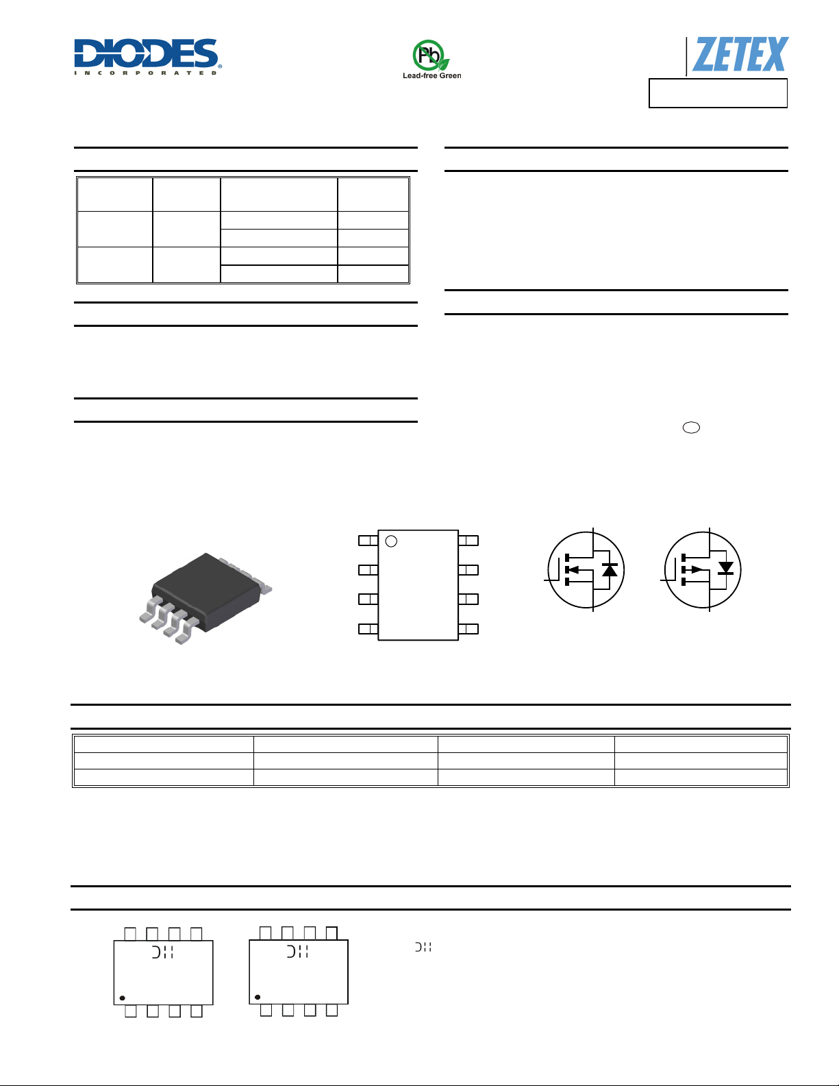
SO-8
Top View
G1
S2
G2
T
A
I
D
= +25C
7.2A
5.4A
-5.2A
-4.7A
Top view
Top View
Low On-Resistance
Fast Switching Speed
Totally Lead-Free & Fully RoHS compliant (Notes 1 & 2)
Halogen and Antimony Free. “Green” Device (Note 3)
Qualified to AEC-Q101 Standards for High Reliability
Mechanical Data
Case: SO-8
Case Material: Molded Plastic, “Green” Molding Compound. UL
Flammability Classification Rating 94V-0
Moisture Sensitivity: Level 1 per J-STD-020
Terminals Connections: See diagram below
Terminals: Finish - Matte Tin annealed over Copper lead frame.
Solderable per MIL-STD-202, Method 208
Weight: 0.074 grams (approximate)
D1
D1S1
D1
1
D2
D2
S1
Q1 N-Channel Q2 P-Channel
Equivalent Circuit
G2
e3
D2
S2
Ordering Information (Note 4)
Part Number Compliance Case Packaging
DMC4028SSD-13 Standard SO-8 2500 / Tape & Reel
DMC4028SSDQ-13 Automotive SO-8 2500 / Tape & Reel
Notes: 1. No purposely added lead. Fully EU Directive 2002/95/EC (RoHS) & 2011/65/EU (RoHS 2) compliant.
2. See http://www.diodes.com/quality/lead_free.html for more information about Diodes Incorporated’s definitions of Halogen- and Antimony-free, "Green"
and Lead-free.
3. Halogen- and Antimony-free "Green” products are defined as those which contain <900ppm bromine, <900ppm chlorine (<1500ppm total Br + Cl) and
<1000ppm antimony compounds.
4. For packaging details, go to our website at http”//www.diodes.com/products/packages.html .
Marking Information
DMC4028SSD
Document Number: D35041 Rev: 2 - 2
C4028SD
YY WW
C4028DQ
YY WW
= Manufacturer’s Marking
C4028SD = Product Type Marking Code for DMC4028SSD-13
C4028DQ = Product Type Marking Code for DMC4028SSDQ-13
YYWW = Date Code Marking
YY = Year (ex: 09 = 2009)
WW = Week (01 - 53)
1 of 11
www.diodes.com
April 2013
© Diodes Incorporated

f
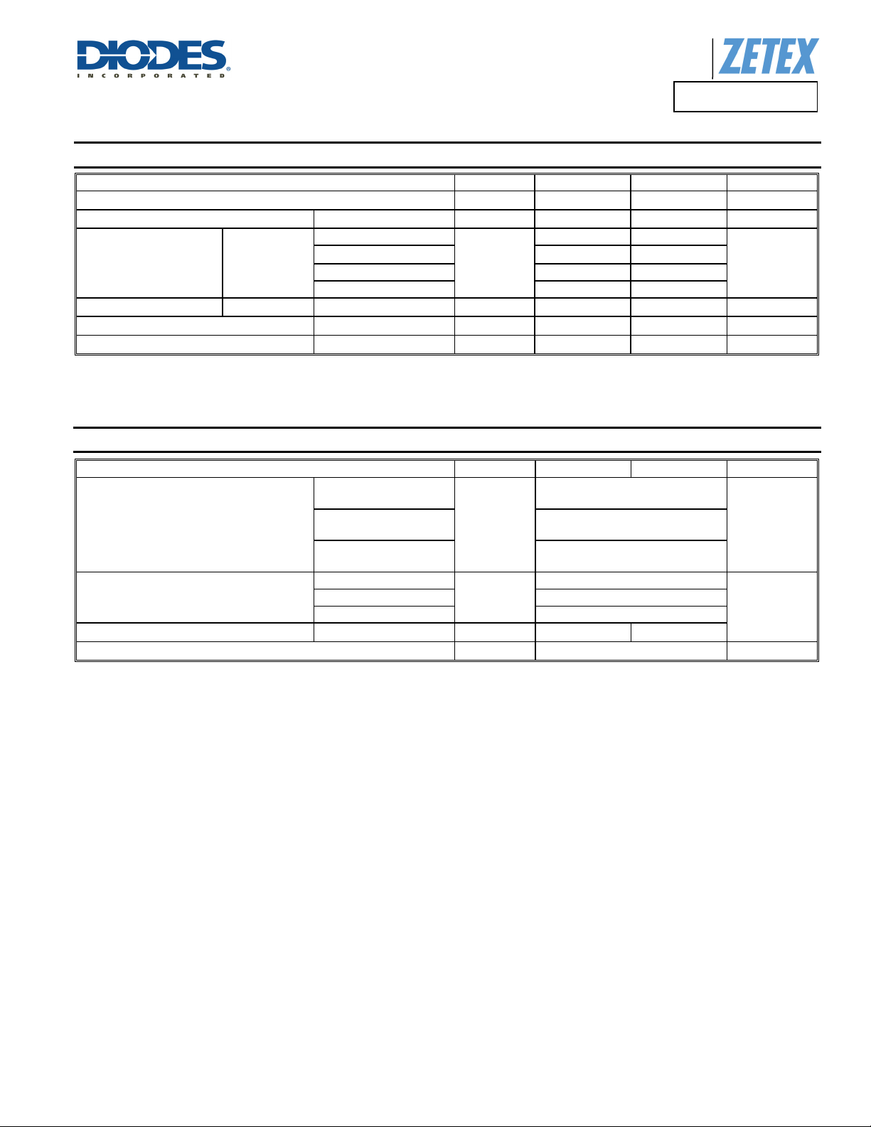
Maximum Ratings (@T
Drain-Source Voltage
Gate-Source Voltage (Note 5)
Continuous Drain Current
Pulsed Drain Current
Continuous Source Current (Body diode) (Notes 7 & 9)
Pulsed Source Current (Body diode) (Notes 8 & 9)
ADVANCE INFORMATION
Thermal Characteristics (@T
= +25°C, unless otherwise specified.)
A
Characteristic Symbol N-Channel - Q1 P-Channel - Q2 Units
V
= 10V
GS
V
= 10V
GS
A
A Product Line o
Diodes Incorporated
V
DSS
V
GSS
(Notes 7 & 9)
TA = 70°C (Notes 7 & 9)
(Notes 6 & 9) 5.4 4
(Notes 6 & 10) 6.5 4.8
(Notes 7 & 9)
= +25°C, unless otherwise specified.)
ID
IDM
I
S
I
SM
40 -40 V
20 20
7.2 5.2
5.5 4.2
27.3 20.4 A
3.35 3.15 A
27.3 20.4 A
DMC4028SSD
V
A
Characteristic Symbol N-Channel - Q1 P-Channel - Q2 Unit
(Notes 6 & 9)
Power Dissipation
Linear Derating Factor
Thermal Resistance, Junction to Ambient
Thermal Resistance, Junction to Lead (Notes 9 & 11)
Operating and Storage Temperature Range
Notes: 5. AEC-Q101 VGS maximum is 16V.
6. For a device surface mounted on 25mm x 25mm x 1.6mm FR4 PCB with high coverage of single sided 1oz copper, in still air conditions; the device is
measured when operating in a steady-state condition.
7. Same as note (5), except the device is measured at t 10 sec.
8. Same as note (5), except the device is pulsed with D= 0.02 and pulse width 300 µs. The pulse current is limited by the maximum junction temperature.
9. For a dual device with one active die.
10. For a device with two active die running at equal power.
11. Thermal resistance from junction to solder-point (at the end of the drain lead).
(Notes 6 & 10)
(Notes 7 & 9)
(Notes 6 & 9)
(Notes 6 & 10) 70
(Notes 7 & 9) 58
P
R
R
T
J, TSTG
θJA
θJL
D
53 53
1.25
10
1.8
14.3
2.16
17.2
100
-55 to +150 °C
W
mW/°C
°C/W
DMC4028SSD
Document Number: D35041 Rev: 2 - 2
2 of 11
www.diodes.com
April 2013
© Diodes Incorporated

f
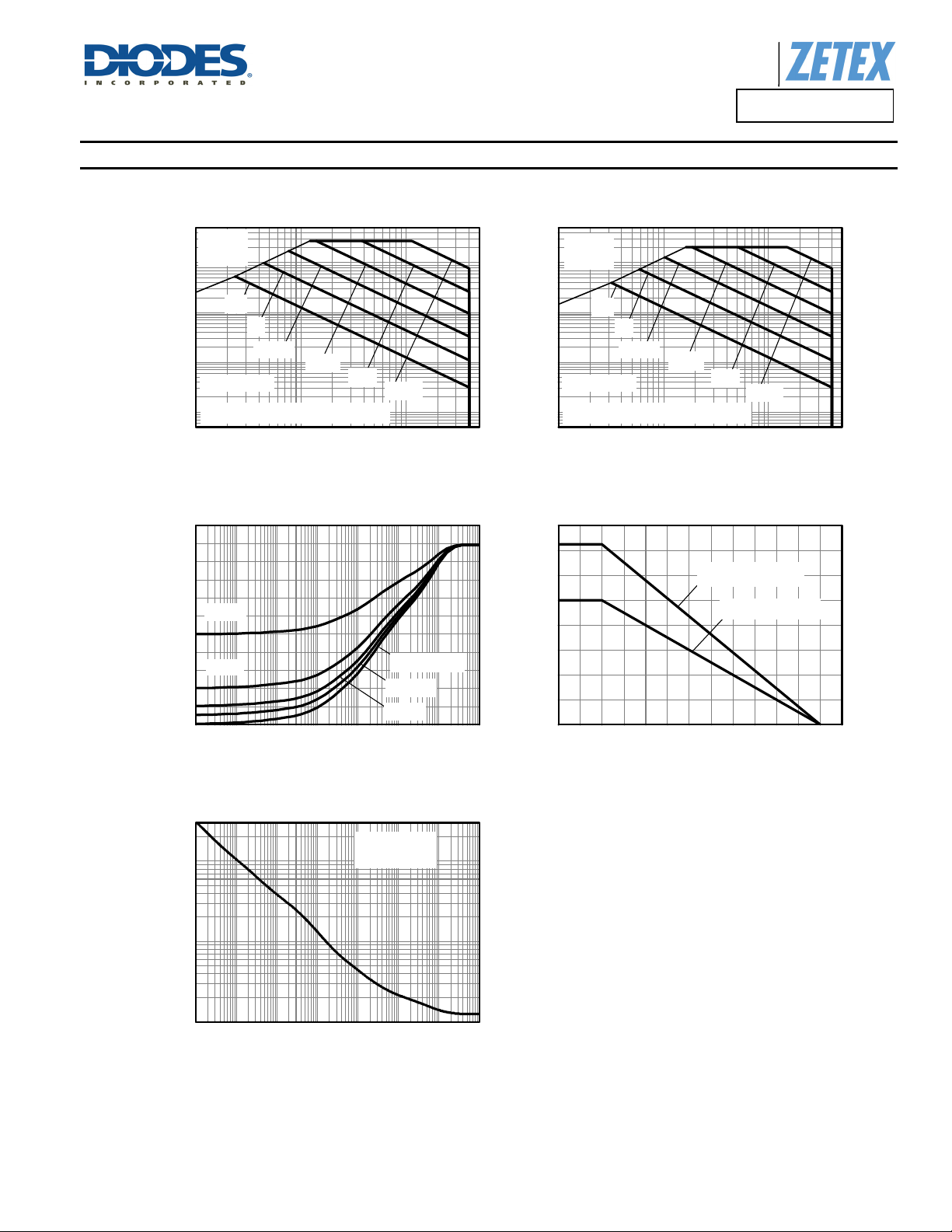
Thermal Characteristics
R
Limited
10
1
100m
(Note 3 & 6)
Drain Current (A)
D
10m
I
NPN @ Single Pulse, T
0.1 1 10
ADVANCE INFORMATION
N-channel Safe Operating Area
DS(ON)
DC
1s
100ms
10ms
amb
1ms
100us
=25°C
VDS Drain-Source Voltage (V)
A Product Line o
Diodes Incorporated
DMC4028SSD
R
DS(ON)
Limited
10
DC
1s
100ms
(Note 3 & 6)
PNP @ Single Pulse, T
0.1 1 10
10ms
amb
1ms
100us
=25°C
100m
Drain Current (A)
D
10m
-I
1
-VDS Drain-Source Voltage (V)
P-channel Safe Operating Area
100
80
D=0.5
60
40
D=0.2
20
Thermal Resistance (°C/W)
0
100µ 1m 10m 100m 1 10 100 1k
Single Pulse
D=0.05
D=0.1
Pulse Width (s)
Transient Thermal Impedance
Single Pulse
=25°C
100
10
T
amb
2.0
1.5
1.0
0.5
0.0
0 25 50 75 100 125 150
Max Power Dissipation (W)
Temperature (°C)
Two active die
One active die
Derating Curve
Maximum Power (W)
1
100µ 1m 10m 100m 1 10 100 1k
Pulse Width (s)
Pulse Power Dissipation
DMC4028SSD
Document Number: D35041 Rev: 2 - 2
3 of 11
www.diodes.com
April 2013
© Diodes Incorporated

f
A Product Line o
Diodes Incorporated
DMC4028SSD
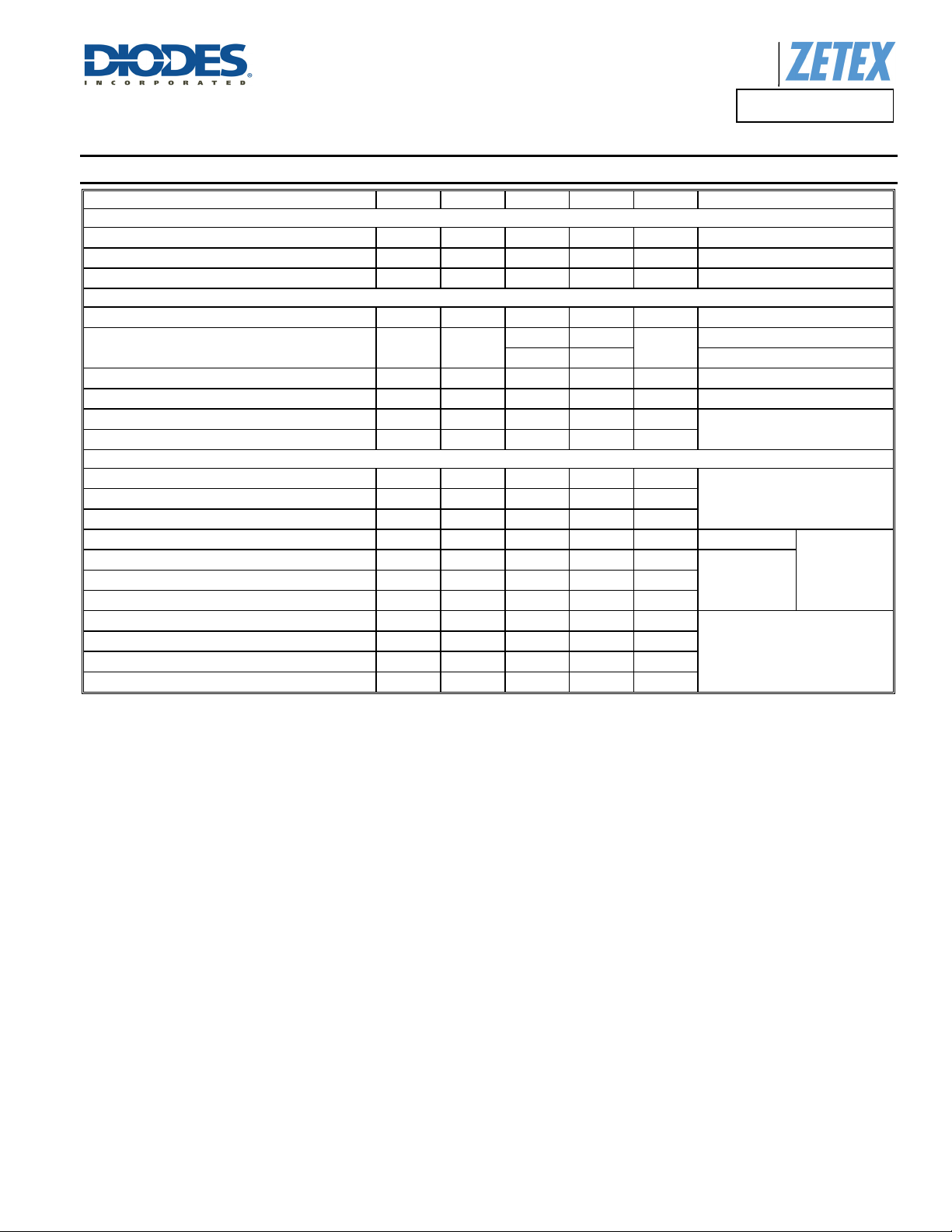
Electrical Characteristics – Q1 N-Channel (@T
Characteristic Symbol Min Typ Max Unit Test Condition
OFF CHARACTERISTICS
Drain-Source Breakdown Voltage
Zero Gate Voltage Drain Current
Gate-Source Leakage
ON CHARACTERISTICS
Gate Threshold Voltage
Static Drain-Source On-Resistance (Note 12)
Forward Transconductance (Notes 12 & 13)
Diode Forward Voltage (Note 12)
Reverse recovery time (Note 13)
Reverse recovery charge (Note 13)
DYNAMIC CHARACTERISTICS (Note 13)
ADVANCE INFORMATION
Input Capacitance
Output Capacitance
Reverse Transfer Capacitance
Total Gate Charge (Note 14)
Total Gate Charge (Note 14)
Gate-Source Charge (Note 14)
Gate-Drain Charge (Note 14)
Turn-On Delay Time (Note 14)
Turn-On Rise Time (Note 14)
Turn-Off Delay Time (Note 14)
Turn-Off Fall Time (Note 14)
Notes: 12. Measured under pulsed conditions. Pulse width 300s; duty cycle 2%
13. For design aid only, not subject to production testing.
14. Switching characteristics are independent of operating junction temperatures.
BV
I
I
V
R
DS (ON)
V
C
C
C
Q
Q
t
D(on)
t
D(off)
DSS
DSS
GSS
GS(th)
g
fs
SD
t
rr
Q
iss
oss
rss
Q
Q
gs
gd
t
r
t
f
rr
g
g
= +25°C, unless otherwise specified.)
A
40
1.0
0.018 0.028
0.033 0.049
22.8
0.845 1.1 V
135
799
604
106
59.6
6.5
12.9
2.3
3.6
4.2
12.4
13.8
10.7
V
0.5 µA
100
nA
3.0 V
Ω
S
ns
nC
pF
pF
pF
nC
nC
nC
nC
ns
ns
ns
ns
ID = 250µA, VGS = 0V
VDS = 40V, VGS = 0V
VGS = 20V, VDS = 0V
ID = 250µA, VDS = VGS
= 10V, ID = 6A
V
GS
V
= 4.5V, ID = 5A
GS
VDS = 15V, ID = 6A
IS = 6A, VGS = 0V
= 6A, di/dt = 100A/s
I
S
V
= 20V, VGS = 0V
DS
f = 1MHz
VGS = 4.5V
V
DS
= 6A
= 10V
V
GS
= 20V, VGS = 10V
V
DD
= 6A, RG 6.0
I
D
I
D
= 20V
DMC4028SSD
Document Number: D35041 Rev: 2 - 2
4 of 11
www.diodes.com
April 2013
© Diodes Incorporated
 Loading...