

Page 1
A
f
20V COMPLEMENTARY PAIR ENHANCEMENT MODE MOSFET
Product Summary
Max
I
D
Device
Q1 20V
Q2 -20V
V
(BR)DSS
R
20mΩ @ V
28mΩ @ VGS = 2.5V
33mΩ @ V
45mΩ @ VGS = -2.5V
DS(on)
max
GS
GS
= 4.5V
= -4.5V
TA = 25°C
(Notes 3 & 5)
8.5A
7.2A
-6.8A
-5.8A
Description and Applications
This MOSFET has been designed to minimize the on-state resistance
) and yet maintain superior switching performance, making it
(R
DS(on)
ideal for high efficiency power management applications.
• Motor control
• DC-DC Converters
• Power management functions
• Notebook Computers and Printers
ESD PROTECTED TO 2kV
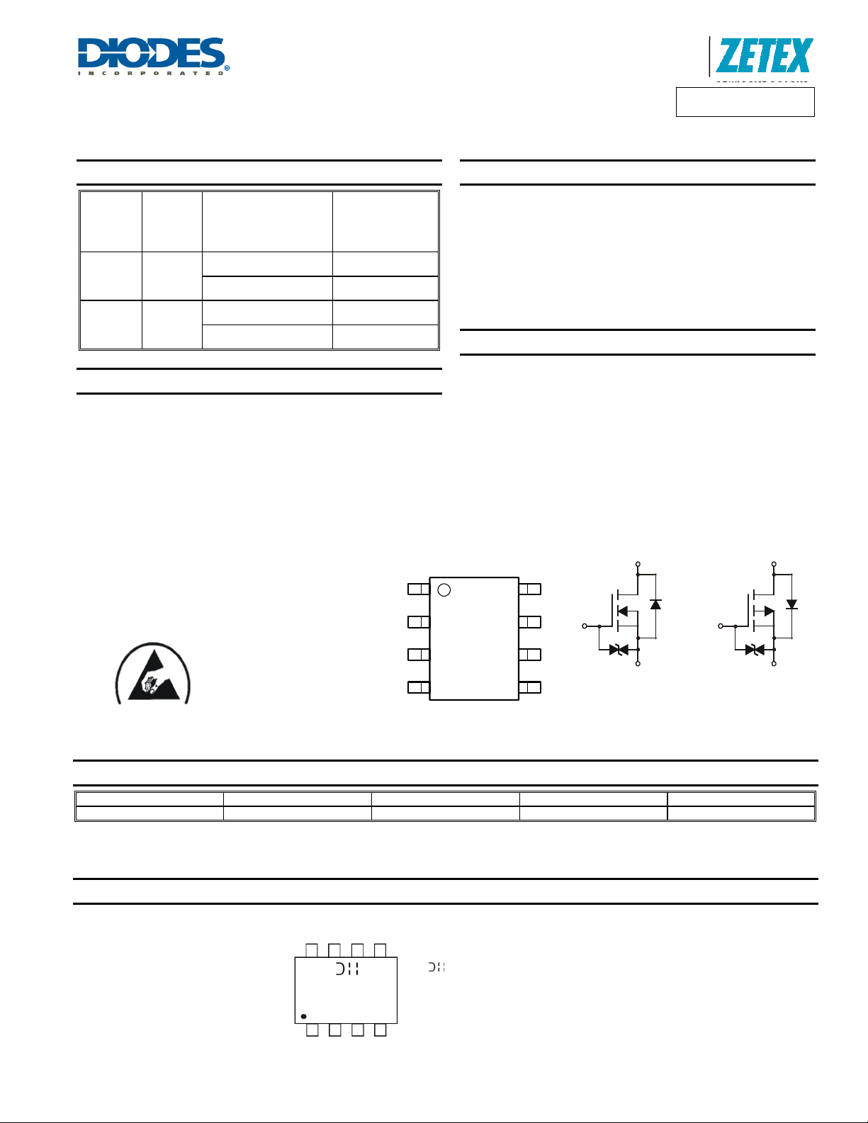
SO-8
G1
S2
G2
Top View
Product Line o
Diodes Incorporated
DMC2020USD
Features and Benefits
• Reduced footprint with two discretes in a single SO8
• Low gate drive
• Low input capacitance
• Fast Switching Speed
• Low Input/Output Leakage
• ESD Protected up to 2kV
• “Lead Free”, RoHS Compliant (Note 1)
• Halogen and Antimony Free. "Green" Device (Note 1)
Mechanical Data
• Case: SO-8
• Case Material: Molded Plastic, “Green” Molding Compound.
UL Flammability Classification Rating 94V-0
• Moisture Sensitivity: Level 1 per J-STD-020
• Terminals Connections: See Diagram
• Terminals: Finish - Matte Tin annealed over Copper lead frame.
Solderable per MIL-STD-202, Method 208
• Weight: 0.074 grams (approximate)
Top View
D1S1
D1
D2
D2
Drain
Body
Gate
Gate
Protection
Diode
Q1 N-Channel Q2 P-Channel
Diode
Source
Equivalent Circuit
Gate
Gate
Protection
Diode
Drain
Source
Body
Diode
Ordering Information (Note 1)
Product Marking Reel size (inches) Tape width (mm) Quantity per reel
DMC2020USD-13 C2020UD 13 12 2,500
Notes: 1. No purposefully added lead. Diodes Inc.'s "Green" policy and packaging details can be found on our website at http://www.diodes.com.
Marking Information
DMC2020USD
Document number: DS32121 Rev. 4 - 2
C2020UD
YY
WW
= Manufacturer’s Marking
C2020UD = Product Type Marking Code
YYWW = Date Code Marking
YY = Year (ex: 09 = 2009)
WW = Week (01 - 53)
www.diodes.com
1 of 11
February 2011
© Diodes Incorporated
Page 2
A
f
Product Line o
Diodes Incorporated
DMC2020USD
Maximum Ratings @T
= 25°C unless otherwise specified
A
Characteristic Symbol N-Channel - Q1 P-Channel - Q2 Units
Drain-Source Voltage
Gate-Source Voltage
(Notes 3 & 5)
Continuous Drain Current
V
GS
= 4.5V
TA = 70°C (Notes 3 & 5)
(Notes 2 & 5) 6.5 -5.2
(Notes 2 & 6) 7.8 -6.3
Pulsed Drain Current
V
GS
= 4.5V
(Notes 4 & 5)
Continuous Source Current (Body diode) (Notes 3 & 5)
Pulsed Source Current (Body diode) (Notes 4 & 5)
V
V
DSS
GSS
ID
IDM
I
S
I
SM
20 -20
±10 ±10
8.5 -6.8
6.8 -5.4
33.6 -26.8
4.0 -4.0
33.6 -26.8
V
A
Thermal Characteristics @T
= 25°C unless otherwise specified
A
Characteristic Symbol N-Channel - Q1 P-Channel - Q2 Unit
(Notes 2 & 5)
Power Dissipation
Linear Derating Factor
(Notes 2 & 6)
P
D
(Notes 3 & 5)
(Notes 2 & 5)
Thermal Resistance, Junction to Ambient
(Notes 2 & 6)
R
θJA
(Notes 3 & 5)
Thermal Resistance, Junction to Lead (Notes 5 & 7)
Operating and Storage Temperature Range
Notes: 2. For a device surface mounted on 25mm x 25mm x 1.6mm FR4 PCB with high coverage of single sided 1oz copper, in still air conditions; the device is
measured when operating in a steady-state condition.
3. Same as note (2), except the device is measured at t ≤ 10 sec.
4. Same as note (2), except the device is pulsed with D = 0.02 and pulse width 300µs.
5. For a dual device with one active die.
6. For a device with two active die running at equal power.
7. Thermal resistance from junction to solder-point (at the end of the drain lead).
R
T
J, TSTG
θJL
1.25
10
1.8
14.3
W
mW/°C
2.14
17.2
100
70
58
°C/W
51
-55 to +150 °C
DMC2020USD
Document number: DS32121 Rev. 4 - 2
2 of 11
www.diodes.com
February 2011
© Diodes Incorporated
Page 3
A
f
Thermal Characteristics
Product Line o
Diodes Incorporated
DMC2020USD
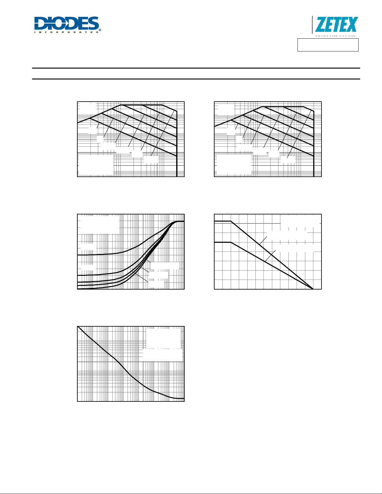
R
DS(ON)
Limited
10
DC
1
100m
Drain Current (A)
D
I
10m
0.1 1 10
1s
100ms
Single Pulse
T
= 25°C
amb
One active die
10ms
1ms
100us
VDS Drain-Source Voltage (V)
N-channel Safe Operating Area
25 mm x 25 mm
100
1oz FR4
One active die
80
D=0.5
60
40
D=0.2
20
Thermal Resistance (°C/W)
0
100µ 1m 10m 100m 1 10 100 1k
Pulse Width ( s)
Single Pulse
D=0.05
D=0.1
R
DS(ON)
Limited
10
DC
1
100m
Drain Current (A)
D
10m
-I
0.1 1 10
1s
100ms
Single Pulse
T
= 25°C
amb
One active die
10ms
1ms
100us
-VDS Drain - So urce Voltage (V)
P-channel Safe Operating A rea
2.0
1.5
1.0
0.5
0.0
0 25 50 75 100 125 150
Max Power Dissipation (W)
Temperature (°C)
25 mm x 25 mm
1oz FR4
Two active die
One active die
Transient Thermal Impedance
Single Pulse
T
100
10
amb
One active die
25 mm x 25 mm
1oz FR4
= 25°C
Deratin g C u rve
Maximum Power (W)
1
100µ 1m 10m 100m 1 10 100 1k
Pulse Width ( s)
Pulse Power Dissipation
DMC2020USD
Document number: DS32121 Rev. 4 - 2
3 of 11
www.diodes.com
© Diodes Incorporated
February 2011
Page 4
A
f
)
g
g
g
g
g
r
R
C
U
R
R
T
R
C
U
R
R
T
Electrical Characteristics – Q1 N-CHANNEL @T
OFF CHARACTERISTICS
Drain-Source Breakdown Voltage
Zero Gate Voltage Drain Current
Gate-Source Leakage
ON CHARACTERISTICS
Gate Threshold Voltage
Static Drain-Source On-Resistance (Note 8)
Forward Transfer Admittance (Notes 8 & 9)
Diode Forward Voltage (Note 8)
Continuous Source Current
DYNAMIC CHARACTERISTICS (Note 9)
Input Capacitance
Output Capacitance
Reverse Transfer Capacitance
Gate Resistance
Total Gate Charge (Note 10)
Total Gate Charge (Note 10)
Gate-Source Charge (Note 10)
Gate-Drain Charge (Note 10)
Turn-On Delay Time (Note 10)
Turn-On Rise Time (Note 10)
Turn-Off Delay Time (Note 10)
Turn-Off Fall Time (Note 10)
Notes: 8. Measured under pulsed conditions. Pulse width ≤ 300μs; duty cycle ≤ 2%
9. For design aid only, not subject to production testing.
10. Switching characteristics are independent of operating junction temperatures.
Characteristic Symbol Min Typ Max Unit Test Condition
BV
DSS
I
DSS
I
GSS
V
GS(th
R
DS (ON)
|Y
|
fs
V
SD
I
S
C
iss
C
oss
C
rss
R
Q
Q
Q
s
Q
d
t
D(on)
t
t
D(off)
t
f
Product Line o
Diodes Incorporated
DMC2020USD
= 25°C unless otherwise specified
A
20 - - V
- - 1.0
- - ±10
0.5 1.1 1.5 V
-
13 20
18 28
- 16 - S
- 0.7 1.2 V
- - 1.8 A -
- 1149 -
- 157 -
- 142 -
- 1.51 -
- 6.0 -
- 11.6 -
- 2.7 -
- 3.4 -
11.67
-
12.49
-
35.89
-
12.33
-
-
-
-
-
VGS = 0V, ID = 250μA
μA
VDS = 20V, VGS = 0V
μA
VGS = ±10V, VDS = 0V
VDS = VGS, ID = 250μA
V
= 4.5V, ID = 7A
mΩ
GS
V
= 2.5V, ID = 3A
GS
VDS = 5V, ID = 9.4A
VGS = 0V, IS = 1.3A
V
= 10V, VGS = 0V,
pF
DS
f = 1.0MHz
Ω
VDS = 0V, VGS = 0V, f = 1MHz
VGS = 2.5V
nC
ns
= 4.5V
V
GS
V
= 4.5V, VDS = 10V,
GS
= 6Ω , I
R
G
= 1A
D
V
DS
I
= 9.4A
D
= 10V
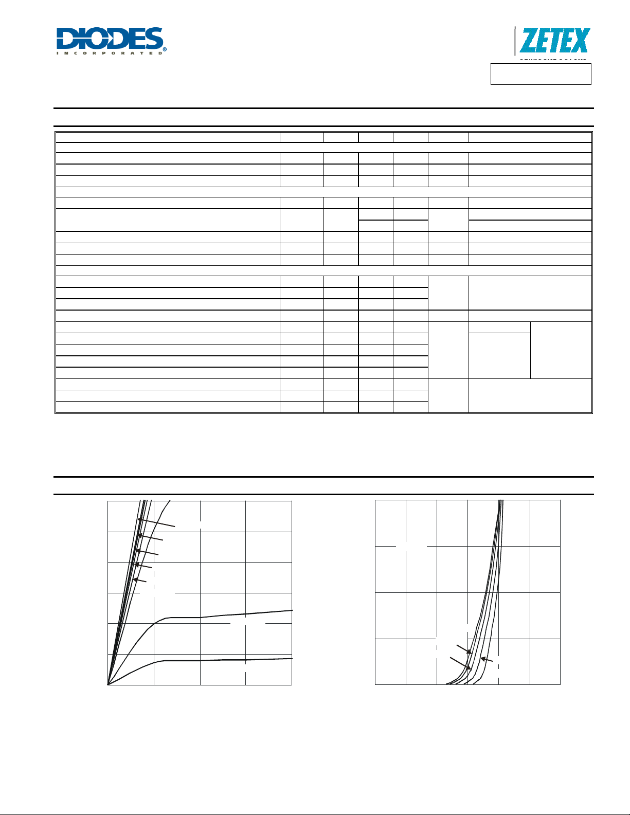
Typical Characteristics – Q1 N-CHANNEL
30
V = 10V
V = 4.5V
GS
V = 4.0V
GS
V = 3.5V
GS
GS
GS
V = 2.0V
GS
(A)
EN
AIN
D
I, D
25
20
15
10
V = 3.0V
V = 2.5V
GS
5
V = 1.8V
GS
0
0 0.5 1 1.5 2
V , DRAIN-SOURCE VOLT AGE (V)
DS
Fig. 1 Typical Output Character i stics
DMC2020USD
Document number: DS32121 Rev. 4 - 2
4 of 11
www.diodes.com
20
15
V = 5V
DS
(A)
EN
10
AIN
T = 150°C
D
I, D
5
0
0 0.5 1 1.5 2 2.5 3
V , GATE SOURCE VOLTAGE (V)
GS
A
T = 125°C
A
T = 85°C
A
T = 25°C
A
T = -55°C
A
Fig. 2 Typical Transfer Characteristics
February 2011
© Diodes Incorporated
Page 5

A
f
R
RAIN-SOUR
CE O
N
R
T
N
C
R
R
OUR
CE ON-R
TANC
O
URC
C
URREN
T
Product Line o
Ω
0.04
Ω
0.04
E ( )
A
0.03
0.03
ESIS
-
Diodes Incorporated
V = 4.5V
GS
DMC2020USD
0.02
V = 2.5V
GS
0.01
DS(ON)
R , DRAIN-SOURCE ON-RESISTANCE ( )
0
0 5 10 15 20 25 30
I , DRAIN-SOURCE CURRENT (A)
D
Fig. 3 Typical On-Resistance
V = 4.5V
GS
vs. Drain C urrent and G ate V o l t age
1.6
1.4
1.2
V = 4.5V
1.0
GS
I = 10A
D
DS(ON)
R , DRAIN-SOURCE
0.8
ON-RESISTANCE (NORMALIZED)
V = 2.5V
GS
I = 5A
D
0.02
0.01
, D
DS(ON)
T = 150°C
A
T = 125°C
A
T = 85°C
T = 25°C
T = -55°C
0
0 5 10 15 20
I , DRAIN CURRENT (A)
D
Fig. 4 Typical Drain-Source On-Resistance
vs. Drain C urrent and Tem per ature
0.04
Ω
E ( )
0.03
ESIS
V = 2.5V
GS
I = 5A
D
V = 4.5V
GS
I = 10A
D
AIN-S
, D
0.02
0.01
A
A
A
0.6
-50 -25 0 25 50 75 100 125 150
T , JUNCTION TEMPERATURE (°C)
J
Fig. 5 On- Resistance Variation with Temperature
1.6
1.4
1.2
I = 1mA
1.0
0.8
I = 250µA
D
D
0.6
0.4
0.2
GS(TH)
V , GATE THRESHOLD VOLTAGE (V)
0
-50 -25 0 25 50 75 100 125 150
T , AMBIENT TEMPERATURE (°C)
A
Fig. 7 Gate Threshold Variation vs. Ambient T emperature
DMC2020USD
Document number: DS32121 Rev. 4 - 2
5 of 11
www.diodes.com
DS(ON)
0
-50 -25 0 25 50 75 100 125 150
T , JUNCTION TEMPERATURE (°C)
J
Fig. 6 On- Resistance Variation with Temperatu r e
30
25
(A)
20
15
E
T = 25°C
A
10
S
I, S
5
0
0 0.2 0.4 0.6 0.8 1.0 1.2
V , SOURCE-DRAIN VOLTAGE (V)
SD
Fig. 8 Diode Forward Voltage vs. Current
February 2011
© Diodes Incorporated
Page 6

A
f
C, CAPACITANC
F
R
N-SOUR
C
GE C
URREN
T
T
OUR
C
OLTAG
G
Product Line o
Diodes Incorporated
DMC2020USD
10,000
)
1,000
E (p
f = 1MHz
C
iss
100,000
(nA)
10,000
1,000
T = 150°C
A
C
oss
C
100
10
048121620
rss
V , DRAIN-SOURCE VOLTAGE (V)
DS
Fig. 9 Typical Capacitance
10
V = 10V
8
E(V)
DS
I = 9.4A
D
6
E V
4
E-S
2
GS
V, A
T = 125°C
E LEAKA
100
10
AI
DSS
1
I, D
0 5 10 15 20
V , DRAIN-SOURCE VOLTAGE (V)
DS
Fig. 10 Typical Drain-Source Leakage Current
A
T = 85°C
A
T = 25°C
A
vs. Drain-S ource Voltage
0
0 5 10 15 20 25
Q , OTAL GATE CHARGE (nC)
T
g
Fig. 11 Gate-Source Voltage vs. Total Gate Charge
DMC2020USD
Document number: DS32121 Rev. 4 - 2
6 of 11
www.diodes.com
February 2011
© Diodes Incorporated
Page 7

A
f
)
g
g
g
g
g
r
R
N
CUR
R
N
T
RAIN CUR
R
N
T
Product Line o
Diodes Incorporated
DMC2020USD
Electrical Characteristics – Q2 P-CHANNEL
@TA
Characteristic Symbol Min Typ Max Unit Test Condition
OFF CHARACTERISTICS
Drain-Source Breakdown Voltage
Zero Gate Voltage Drain Current
Gate-Source Leakage
BV
I
DSS
I
GSS
DSS
ON CHARACTERISTICS (Note 7)
Gate Threshold Voltage
Static Drain-Source On-Resistance (Note 11)
Forward Transfer Admittance (Note 11 & 12)
Diode Forward Voltage (Note 11)
Continuous Source Current
V
GS(th
R
DS (ON)
|Y
V
|
fs
SD
I
S
DYNAMIC CHARACTERISTICS (Note 12)
Input Capacitance
Output Capacitance
Reverse Transfer Capacitance
Gate Resistance
Total Gate Charge (Note 13)
Total Gate Charge (Note 13)
Gate-Source Charge (Note 13)
Gate-Drain Charge (Note 13)
Turn-On Delay Time (Note 13)
Turn-On Rise Time (Note 13)
Turn-Off Delay Time (Note 13)
Turn-Off Fall Time (Note 13)
Notes: 11. Measured under pulsed conditions. Pulse width ≤ 300μs; duty cycle ≤ 2%
12. For design aid only, not subject to production testing.
13. Switching characteristics are independent of operating junction temperatures.
C
C
C
R
Q
Q
Q
Q
t
D(on)
t
D(off)
iss
oss
rss
t
t
s
d
f
= 25°C unless otherwise specified
-20 - - V
- - -1.0
- - ±10
-0.4 -0.7 -1.0 V
-
26 33
33 45
- 14 - S
- -0.7 -1.0 V
VGS = 0V, ID = -250μA
μA
μA
= -20V, VGS = 0V
V
DS
= ±8V, VDS = 0V
V
GS
VDS = VGS, ID = -250μA
V
= -4.5V, ID = -6A
mΩ
GS
V
= -2.5V, ID = -3A
GS
VDS = -5V, ID = -4A
VGS = 0V, IS = -1A
- - -1.8 A -
- 1610 -
- 157 -
- 145 -
- 9.45 -
- 8.0 -
- 15.4 -
- 2.5 -
pF
Ω
nC
= -10V, VGS = 0V,
V
DS
f = 1.0MHz
= 0V, VGS = 0V, f = 1MHz
V
DS
VGS = -2.5V
V
V
GS
= -4.5V
I
D
- 3.3 -
16.8
-
12.4
-
94.1
-
42.4
-
-
-
-
ns
V
= -4.5V, VDS = -10V,
GS
R
= 6Ω , ID = -1A
G
-
= -10V
DS
= -4A
Typical Characteristics – Q2 P-CHANNEL
30
V = -3.5V
25
(A)
20
E
15
V = -10V
GS
V = -4.5V
GS
V = -4.0V
GS
V = -2.5V
V = -3.0V
GS
GS
GS
V = -2.0V
GS
AI
10
D
-I , D
V = -1.8V
GS
5
0
0 0.5 1.0 1.5 2.0
-V , DRAIN-SOURCE VOLTAGE (V)
DS
Fig. 12 Typical Output Characteristics
DMC2020USD
Document number: DS32121 Rev. 4 - 2
7 of 11
www.diodes.com
20
V = -5V
DS
15
(A)
E
10
D
-I , D
5
0
0 0.5 1 1.5 2 2.5 3
T = 150°C
A
T = 125°C
A
T = 85°C
A
-V , GATE SOURCE VOLTAGE (V)
GS
T = 25°C
A
T = -55°C
A
Fig. 13 Typical Transfer Characteristics
February 2011
© Diodes Incorporated
Page 8

A
f
R
R
OUR
CE ON-R
TANC
R
RAIN-SOUR
CE O
N-R
T
N
C
R
R
OUR
C
R
R
OUR
CE ON-R
TANC
2
GAT
T
H
RESH
O
OLT
G
OUR
C
CUR
R
T
Product Line o
Ω
E ( )
0.06
0.05
0.06
Ω
E ( )
0.05
A
Diodes Incorporated
V = 4.5V
GS
DMC2020USD
0.04
ESIS
-V = 2.5V
0.03
GS
-V = 4.5V
GS
0.02
AIN-S
, D
0.01
DS(ON)
0
0 5 10 15 20 25 30
-I , DRAIN-SOURCE CURRENT (A)
D
Fig. 14 Typical On-Resistance
vs. Drain C ur r ent and G at e Voltage
1.6
1.4
E
1.2
AIN-S
, D
DS(ON)
-V = 4.5V
GS
-I = 10A
ON-RESISTANCE (NORMALIZED)
1.0
0.8
0.6
D
-V = 2.5V
GS
-I = 5A
D
-50 -25 0 25 50 75 100 125 150
T , JUNCTION TEMPERATURE (°C)
J
Fig. 16 On-Resistance Variation with T emperature
1.
0.04
ESIS
0.03
0.02
0.01
, D
DS(ON)
0
0 5 10 15 20
-I , DRAIN CURRENT (A)
D
T = 150°C
A
T = 125°C
A
T = 85°C
A
T = 25°C
A
T = -55°C
A
Fig. 15 Typical Drain-Source On-Resistance
vs. Drain Current and Temperature
0.06
Ω
E ( )
0.05
ESIS
0.04
-V = 2.5V
GS
-I = 5A
D
0.03
-V = 4.5V
GS
-I = 10A
D
AIN-S
, D
DS(ON)
0.02
0.01
0
-50 -25 0 25 50 75 100 125 150
T , JUNCTION TEMPERATURE (°C)
J
Fig. 17 On-Resistance Variation with Temperature
30
E (V)
1.0
25
A
(A)
0.8
LD V
0.6
E
0.4
-I = 250µA
D
-I = 1mA
D
0.2
GS(TH)
V,
0
-50 -25 0 25 50 75 100 125 150
T , AMBIENT TEMPERATURE (°C)
A
Fig. 18 Gate Threshold Variation vs. Ambient Temperature
DMC2020USD
Document number: DS32121 Rev. 4 - 2
8 of 11
www.diodes.com
20
EN
15
E
10
S
-I , S
5
0
0 0.2 0.4 0.6 0.8 1.0 1.2
-V , SOURCE-DRAIN VOLTAGE (V)
SD
Fig. 19 Diode Forward Voltage vs. Current
T = 25°C
A
February 2011
© Diodes Incorporated
Page 9

A
f
C, CAP
C
TANC
F
R
OUR
C
G
C
URRENT
Product Line o
10,000
f = 1MHz
100,000
(nA)
Diodes Incorporated
DMC2020USD
)
C
1,000
E (p
iss
I
A
100
10
048121620
-V , DRAIN-SOURCE VOLTAGE (V)
C
oss
C
rss
DS
Fig. 20 Typical Capacitance
10
V = -10V
8
DS
I = -4A
D
6
10,000
T = 150°C
A
E
1,000
E LEAKA
100
10
AIN-S
DSS
1
-I , D
0 5 10 15 20
-V , DRAIN-SOURCE VOLTAGE (V)
DS
Fig. 21 Typical Drain-Source Leakage Current
vs. Drain-Source Voltage
T = 125°C
A
T = 85°C
A
T = 25°C
A
4
G
GS
2
-V , ATE-SOURCE VOLTAGE (V)
0
0 5 10 15 20 25 30 35
T
Q , OTAL GATE CHARGE (nC)
g
Fig. 22 Gate-Source Voltage vs. Total Gate Charge
DMC2020USD
Document number: DS32121 Rev. 4 - 2
9 of 11
www.diodes.com
February 2011
© Diodes Incorporated
Page 10

A
f
0
Package Outline Dimensions
DIM Inches Millimeters DIM Inches Millimeters
Product Line o
Diodes Incorporated
DMC2020USD
h x 45°
Min. Max. Min. Max. Min. Max. Min.
Max.
A 0.053 0.069 1.35 1.75 e 0.050 BSC 1.27 BSC
A1 0.004 0.010 0.10 0.25 b 0.013 0.020 0.33 0.51
D 0.189 0.197 4.80 5.00 c 0.008 0.010 0.19 0.25
H 0.228 0.244 5.80 6.20
θ
0° 8° 0° 8°
E 0.150 0.157 3.80 4.00 h 0.010 0.020 0.25 0.50
L 0.016 0.050 0.40 1.27 - - - - -
Suggested Pad Layout
DMC2020USD
Document number: DS32121 Rev. 4 - 2
7.0
0.275
0.6
.024
10 of 11
www.diodes.com
1.52
0.060
4.0
0.155
0.050
1.27
inches
mm
February 2011
© Diodes Incorporated
Page 11

A
f
Product Line o
IMPORTANT NOTICE
DIODES INCORPORATED MAKES NO WARRANTY OF ANY KIND, EXPRESS OR IMPLIED, WITH REGARDS TO THIS DOCUMENT,
INCLUDING, BUT NOT LIMITED TO, THE IMPLIED WARRANTIES OF MERCHANTABILITY AND FITNESS FOR A PARTICULAR PURPOSE
(AND THEIR EQUIVALENTS UNDER THE LAWS OF ANY JURISDICTION).
Diodes Incorporated and its subsidiaries reserve the right to make modifications, enhancements, improvements, corrections or other changes
without further notice to this document and any product described herein. Diodes Incorporated does not assume any liability arising out of the
application or use of this document or any product described herein; neither does Diodes Incorporated convey any license under its patent or
trademark rights, nor the rights of others. Any Customer or user of this document or products described herein in such applications shall assume
all risks of such use and will agree to hold Diodes Incorporated and all the companies whose products are represented on Diodes Incorporated
website, harmless against all damages.
Diodes Incorporated does not warrant or accept any liability whatsoever in respect of any products purchased through unauthorized sales channel.
Should Customers purchase or use Diodes Incorporated products for any unintended or unauthorize d application, Customers shall indemnify and
hold Diodes Incorporated and its representatives harmless against all claims, damages, expenses, and attorney fees arising out of, directly or
indirectly, any claim of personal injury or death associated with such unintended or unauthorized application.
Products described herein may be covered by one or more United States, international or foreign patents pending. Product names and markings
noted herein may also be covered by one or more United States, international or foreign trademarks.
LIFE SUPPORT
Diodes Incorporated products are specifically not authorized for use as critical components in life support devices or systems without the express
written approval of the Chief Executive Officer of Diodes Incorporated. As used herein:
A. Life support devices or systems are devices or systems which:
1. are intended to implant into the body, or
2. support or sustain life and whose failure to perform when properly used in accordance with instructions for use provided in the
labeling can be reasonably expected to result in significant injury to the user.
B. A critical component is any component in a life support device or system whose failure to perform can be reasonably expected to cause the
failure of the life support device or to affect its safety or effectiveness.
Customers represent that they have all necessary expertise in the safety and regulatory ramifications of their life support devices or systems, and
acknowledge and agree that they are solely responsible for all legal, regulatory and safety-related requirements concerning their products and any
use of Diodes Incorporated products in such safety-critical, life support devices or systems, notwithstanding any devices- or systems-related
information or support that may be provided by Diodes Incorporated. Further, Customers must fully indemnify Diodes Incorporated and its
representatives against any damages arising out of the use of Diodes Incorporated products in such safety-critical, life support devices or systems.
Copyright © 2011, Diodes Incorporated
www.diodes.com
Diodes Incorporated
DMC2020USD
DMC2020USD
Document number: DS32121 Rev. 4 - 2
11 of 11
www.diodes.com
February 2011
© Diodes Incorporated
 Loading...