

Page 1
K
Features
• Low On-Resistance
• Low Gate Threshold Voltage V
• Low Input Capacitance
• Fast Switching Speed
• Low Input/Output Leakage
• Complementary Pair MOSFET
• Ultra-Small Surface Mount Package
• Lead Free/RoHS Compliant (Note 2)
• ESD Protected Gate
• "Green" Device (Note 3)
NEW PRODUCT
COMPLEMENTARY PAIR ENHANCEMENT MODE FIELD EFFECT TRANSISTOR
< 1V
GS(th)
ESD protected
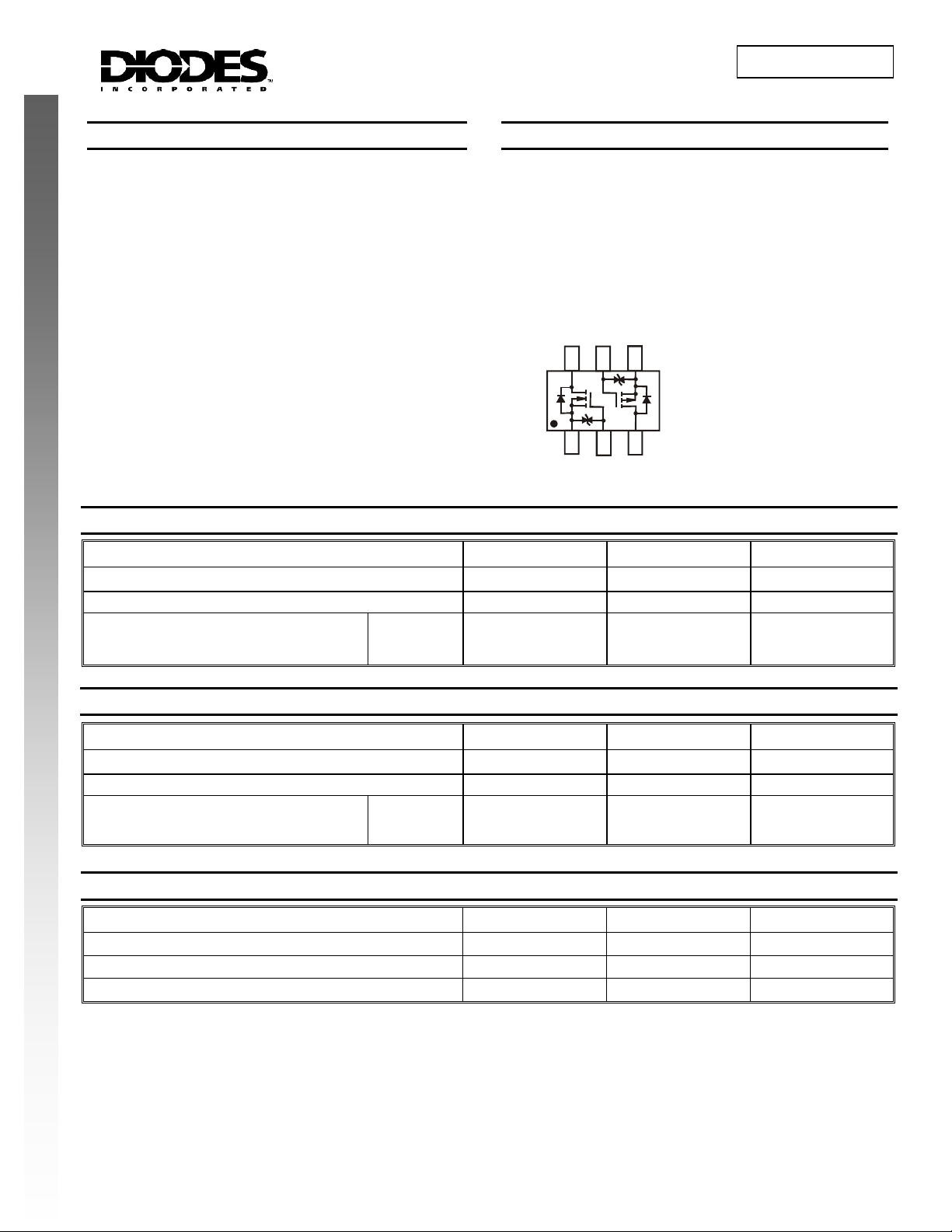
TOP VIEW
DMC2004DW
Mechanical Data
• Case: SOT-363
• Case Material: Molded Plastic. UL Flammability Classification
Rating 94V-0
• Moisture Sensitivity: Level 1 per J-STD-020C
• Terminals: Solderable per MIL-STD-202, Method 208
• Lead Free Plating (Matte Tin Finish annealed over Alloy 42
leadframe).
• Terminal Connections: See Diagram
• Marking Information: See Page 7
• Ordering & Date Code Information: See Page 7
• Weight: 0.006 grams (approximate)
SOT-363
D
1
Q
1
S
1
TOP VIEW
Internal Schematic
G
S
2
2
Q
2
D
G
2
1
Maximum Ratings N-CHANNEL – Q1 @T
= 25°C unless otherwise specified
A
Characteristic Symbol Value Unit
Drain Source Voltage
Gate-Source Voltage
Drain Current (Note 1)
TA = 25°C
= 85°C
T
A
Maximum Ratings P-CHANNEL – Q
@T
2
= 25°C unless otherwise specified
A
Characteristic Symbol Value Unit
Drain Source Voltage
Gate-Source Voltage
= 25°C
T
Drain Current (Note 1)
A
= 85°C
T
A
Thermal Characteristics – Total Device @T
Characteristic Symbol Value Unit
Power Dissipation (Note 1)
Thermal Resistance, Junction to Ambient
Operating and Storage Temperature Range
Notes: 1. Device mounted on FR-4 PCB.
DMC2004DWK
Document number: DS31114 Rev. 4 - 2
2. No purposefully added lead.
3. Diodes Inc.’s “Green” policy can be found on our website at http://www.diodes.com/products/lead_free/index.php.
www.diodes.com
V
DSS
V
GSS
I
D
V
DSS
V
GSS
I
D
= 25°C unless otherwise specified
A
P
d
R
JA
θ
T
, T
j
STG
20 V
±8
540
390
-20 V
±8
-430
-310
250 mW
500
-65 to +150
1 of 8
V
mA
V
mA
°C/W
°C
September 2007
© Diodes Incorporated
Page 2
K
Electrical Characteristics N-CHANNEL – Q
Characteristic Symbol Min Typ Max Unit Test Condition
OFF CHARACTERISTICS (Note 4)
Drain-Source Breakdown Voltage
Zero Gate Voltage Drain Current
Gate-Source Leakage
ON CHARACTERISTICS (Note 4)
Gate Threshold Voltage
Static Drain-Source On-Resistance
Forward Transfer Admittance
Diode Forward Voltage (Note 4)
DYNAMIC CHARACTERISTICS
Input Capacitance
NEW PRODUCT
Output Capacitance
Reverse Transfer Capacitance
Electrical Characteristics P-CHANNEL – Q2 @T
Characteristic Symbol Min Typ Max Unit Test Condition
OFF CHARACTERISTICS (Note 4)
Drain-Source Breakdown Voltage
Zero Gate Voltage Drain Current
Gate-Source Leakage
ON CHARACTERISTICS (Note 4)
Gate Threshold Voltage
Static Drain-Source On-Resistance
Forward Transfer Admittance
Diode Forward Voltage (Note 4)
DYNAMIC CHARACTERISTICS
Input Capacitance
Output Capacitance
Reverse Transfer Capacitance
Notes: 4. Short duration pulse test used to minimize self-heating effect.
DMC2004DWK
Document number: DS31114 Rev. 4 - 2
@T
= 25°C unless otherwise specified
A
1
BV
DSS
I
DSS
I
GSS
V
GS(th)
R
DS (ON)
|Y
V
C
C
C
BV
I
I
V
GS(th)
R
DS (ON)
|Y
V
C
C
C
fs
SD
iss
oss
rss
DSS
DSS
GSS
fs
SD
iss
oss
rss
0.5
200
|
0.5
= 25°C unless otherwise specified
A
-20
-0.5
200
|
-0.5
2 of 8
www.diodes.com
20
⎯ ⎯
⎯ ⎯
⎯ ⎯
⎯
⎯
⎯
⎯
0.4
0.5
0.7
⎯ ⎯
⎯
⎯ ⎯
⎯ ⎯
⎯ ⎯
⎯ ⎯
⎯ ⎯
⎯ ⎯
⎯
0.7
⎯
1.1
1.7
⎯ ⎯
⎯
⎯ ⎯
⎯ ⎯
⎯ ⎯
V
1
μA
± 1 μA
1.0 V
0.55
0.70
Ω
0.90
mS
1.2 V
150 pF
25 pF
20 pF
V
-1.0
μA
± 1.0 μA
-1.0 V
0.9
1.4
Ω
2.0
mS
-1.2 V
175 pF
30 pF
20 pF
DMC2004DW
V
= 0V, ID = 10μA
GS
V
= 16V, VGS = 0V
DS
V
= ±4.5V, VDS = 0V
GS
V
= VGS, ID = 250μA
DS
= 4.5V, ID = 540mA
V
GS
= 2.5V, ID = 500mA
V
GS
V
= 1.8V, ID = 350mA
GS
VDS =10V, ID = 0.2A
V
= 0V, IS = 115mA
GS
V
= 16V, VGS = 0V
DS
f = 1.0MHz
V
= 0V, ID = -250μA
GS
V
= -20V, VGS = 0V
DS
V
= ±4.5V, VDS = 0V
GS
V
= VGS, ID = -250μA
DS
= -4.5V, ID = -430mA
V
GS
= -2.5V, ID = -300mA
V
GS
V
= -1.8V, ID = -150mA
GS
VDS =10V, ID = 0.2A
V
= 0V, IS = -115mA
GS
V
= -16V, VGS = 0V
DS
f = 1.0MHz
September 2007
© Diodes Incorporated
Page 3
K
R
A
CUR
RENT
A
R
A
CUR
R
E
T
A
G
A
R
O
O
A
G
NEW PRODUCT
Q
N-CHANNEL
1,
)
(
IN
D
I, D
0
0
V , DRAI N SOUR C E VOLTAG E (V)
DS
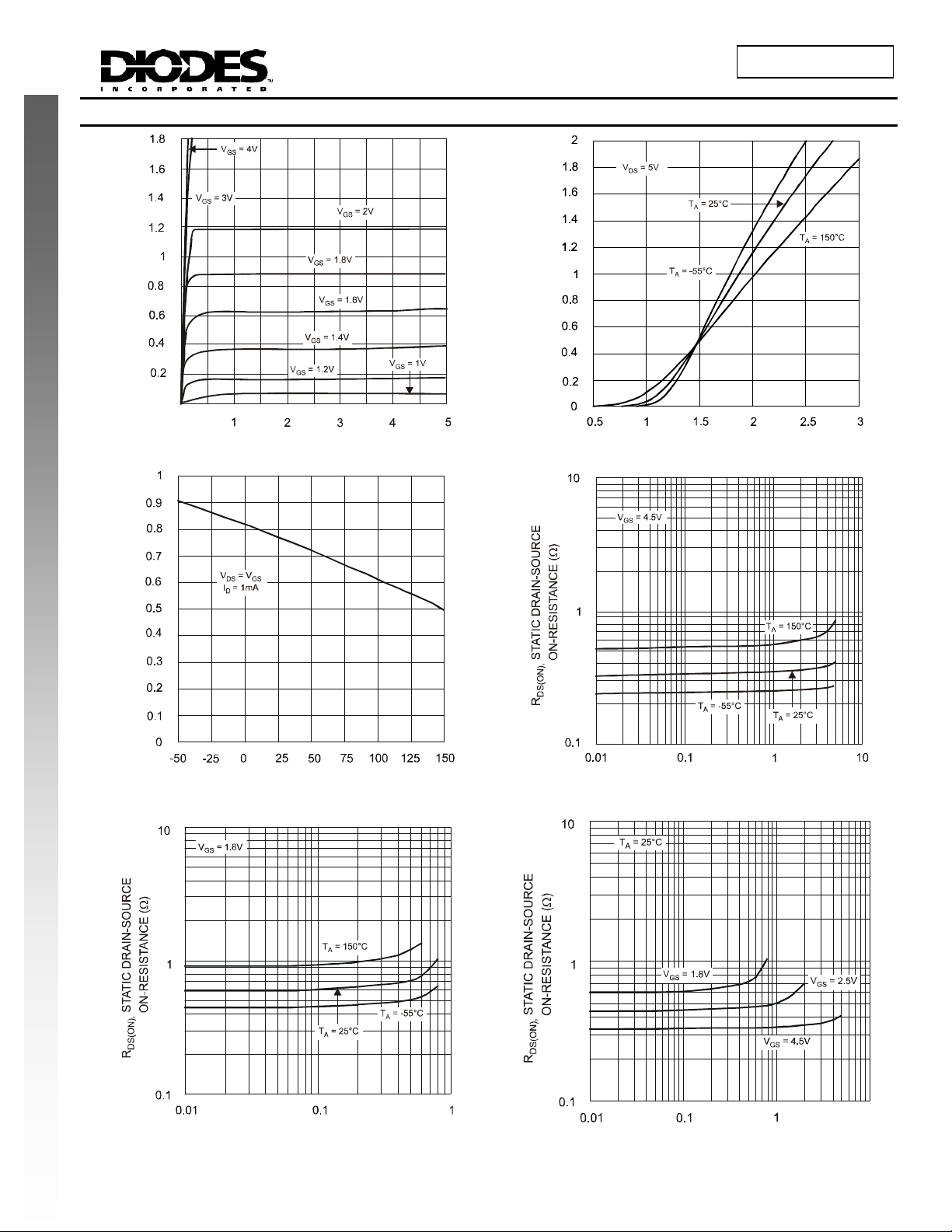
Fig. 1 Typical Output Characteristics
)
(
N
IN
D
I, D
V , GATE SOURCE VOLTAGE (V)
GS
Fig. 2 Typical Transfer Characteristics
DMC2004DW
E (V)
LT
LD V
ESH
TE TH
GS(th)
V,
T , AMBIENT TEMPERATURE (°C)
A
Fig. 3 Gate Threshold Voltage vs.
Ambient Temperat u re
I , DRAIN CURRENT (A)
Fig. 4 Static Drain-Source On-Resistance vs.
D
Drain Curre nt
I , DRAIN CURRENT (A)
Fig. 5 Static Drain-S ource On-Resistance vs.
DMC2004DWK
Document number: DS31114 Rev. 4 - 2
D
Drain Curre nt
3 of 8
www.diodes.com
I , DRAIN-SOURCE CURRENT (A)
D
Fig. 6 Static Drain-Source On-Resistance vs.
Drain-Source Current vs. Gate So ur ce Voltage
September 2007
© Diodes Incorporated
10
Page 4

K
NEW PRODUCT
Q
N-CHANNEL, continued
1,
T , AMBIENT TEMPERATURE (°C)
A
Fig. 7 Static Drain-Source On-State Resistance
vs. Ambi ent Te mpe rature
Fig. 8 Rever se Drain Current vs. So ur ce-Drain Vol t age
V , DRAIN-SOURCE VOLTAGE (V)
SD
DMC2004DW
I , DRAIN CURRENT (A)
D
Fig. 9 Forward Transfer Admittance vs.
DMC2004DWK
Document number: DS31114 Rev. 4 - 2
Drain Cur r ent
4 of 8
www.diodes.com
V , DRAIN-SOURCE VOLTAGE (V)
DS
Fig. 10 Typical Capacitance
September 2007
© Diodes Incorporated
Page 5

K
R
CUR
R
T
R
A
CUR
R
ENT
A
G
A
R
O
O
A
G
NEW PRODUCT
DMC2004DW
Q
P-CHANNEL
2,
(A)
EN
AIN
-I , D
D
0
0
-V , DRAIN SOURCE VOLTAGE (V)
DS
Fig. 11 Typical Output Characteristics
)
(
IN
D
-I , D
-V , GATE SOURCE VOLTAGE (V)
GS
Fig. 12 Typical Transfer Characteristics
E (V)
LT
LD V
ESH
TE TH
GS(th)
-V ,
T , AMBIENT TEMPERATURE (°C)
A
Fig. 13 Gate Threshold Voltage vs.
Ambient Temperat u r e
-I , DRAIN-SOURCE CURRENT (A)
D
Fig. 14 Static Drain-Source On-Resistance vs.
Drain Cur r ent
10
-I , DRAIN-SOURCE CURRENT (A)
D
Fig. 15 Static Drain-Source On-Resistance vs.
DMC2004DWK
Document number: DS31114 Rev. 4 - 2
Drain Curr ent
5 of 8
www.diodes.com
-I , DRAIN-SOURCE CURRENT (A)
D
Fig. 16 Static Drain-Source On-Resistance vs.
Drain-Source Current vs. Gate So ur ce Voltage
September 2007
© Diodes Incorporated
Page 6

K
NEW PRODUCT
Q
P-CHANNEL, Continued
2,
T , AMBIENT TEMPERATURE (°C)
A
Fig. 17 Static Drain-Source On-State Resistance
vs. Ambie nt T emper ature
Fig. 18 Reverse Drain Current vs. Source-Drain Voltage
-V , SOURCE-DRAIN VOLTAGE (V)
DS
DMC2004DW
-I , DRAIN CURRENT (A)
Fig. 19 Forward Transfer Admittance vs. Drain Current
D
DMC2004DWK
Document number: DS31114 Rev. 4 - 2
6 of 8
www.diodes.com
-V , DRAIN-SOURCE VOLTAGE (V)
DS
Fig. 20 Typical Capacitance
September 2007
© Diodes Incorporated
Page 7

K
Ordering Information (Note 5)
Part Number Case Packaging
DMC2004DWK-7 SOT-363 3000/Tape & Reel
Notes: 5. For packaging details, go to our website at http://www.diodes.com/datasheets/ap02007.pdf.
Marking Information
NEW PRODUCT
Date Code Key
Year 2007 2008 2009 2010 2011 2012
Code U V W X Y Z
Month Jan Feb Mar Apr May Jun Jul Aug Sep Oct Nov Dec
Code 1 2 3 4 5 6 7 8 9 O N D
CAB
CAB = Marking Code
YM = Date Code Marking
Y = Year ex: U = 2007
YM
M = Month ex: 9 = September
Package Outline Dimensions
K
J
A
Dim Min Max
B C
H
M
D
L
F
A 0.10 0.30
B 1.15 1.35
C 2.00 2.20
D 0.65 Nominal
F 0.30 0.40
H 1.80 2.20
J
K 0.90 1.00
L 0.25 0.40
M 0.10 0.25
α
All Dimensions in mm
Suggested Pad Layout
G
Z
Y
X
EE
Dimensions Value (in mm)
Z 2.5
G 1.3
X 0.42
Y 0.6
C
C 1.9
E 0.65
SOT-363
⎯
0°
DMC2004DW
0.10
8°
DMC2004DWK
Document number: DS31114 Rev. 4 - 2
7 of 8
www.diodes.com
September 2007
© Diodes Incorporated
Page 8

K
IMPORTANT NOTICE
Diodes Incorporated and its subsidiaries reserve the right to make modifications, enhancements, improvements, corrections or other changes
without further notice to any product herein. Diodes Incorporated does not assume any liability arising out of the application or use of any product
described herein; neither does it convey any license under its patent rights, nor the rights of others. The user of products in such applications shall
assume all risks of such use and will agree to hold Diodes Incorporated and all the companies whose products are represented on our website,
harmless against all damages.
LIFE SUPPORT
Diodes Incorporated products are not authorized for use as critical components in life support devices or systems without the expressed written
approval of the President of Diodes Incorporated.
DMC2004DW
NEW PRODUCT
DMC2004DWK
Document number: DS31114 Rev. 4 - 2
8 of 8
www.diodes.com
September 2007
© Diodes Incorporated
 Loading...