Diodes DMB54D0UDW User Manual

θ
Please click here to visit our online spice models database.
N-CHANNEL ENHANCEMENT MODE MOSFET PLUS PNP TRANSISTOR
Features
• N-Channel MOSFET and PNP Transistor in One Package
• Low On-Resistance
• Very Low Gate Threshold Voltage, 1.0V max
• Low Input Capacitance
• Fast Switching Speed
• Low Input/Output Leakage
• Ultra-Small Surface Mount Package
• Lead, Halogen and Antimony Free, RoHS Compliant (Note
• ESD Protected MOSFET Gate up to 2kV
• "Green" Device (Note 3)
• Qualified to AEC-Q101 Standards for High Reliability
ESD protected gate up to 2kV
2)
SOT-363
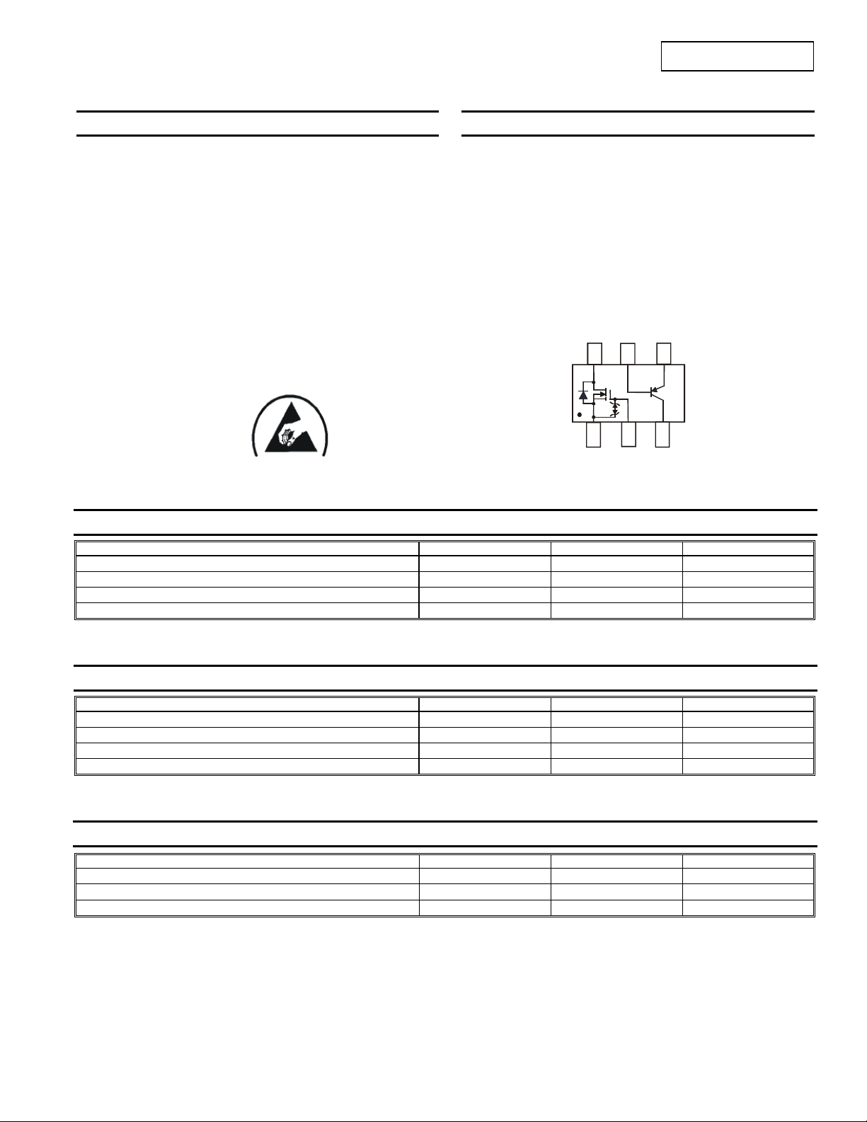
TOP VIEW
DMB54D0UDW
Mechanical Data
• Case: SOT-363
• Case Material: Molded Plastic, “Green” Molding Compound.
UL Flammability Classification Rating 94V-0
• Moisture Sensitivity: Level 1 per J-STD-020
• Terminal Connections: See Diagram
• Terminals: Finish - Matte Tin annealed over Alloy 42 lead frame.
Solderable per MIL-STD-202, Method 208
• Marking Information: See Page 5
• Ordering Information: See Page 5
• Weight: 0.006 grams (approximate)
D
2
Q
1
S
2
TOP VIEW
Internal Schematic
E
B
Q
2
G
C
2
Maximum Ratings – MOSFET, Q1 @T
Characteristic Symbol Value Units
Drain-Source Voltage
Gate-Source Voltage
Drain Current (Note 1) Continuous
Pulsed Drain Current (Note 1)
Maximum Ratings - PNP Transistor, Q2 @T
Characteristic Symbol Value Unit
Collector-Base Voltage
Collector-Emitter Voltage
Emitter-Base Voltage
Collector Current
Thermal Characteristics, Total Device @T
Characteristic Symbol Value Unit
Total Power Dissipation (Note 1)
Thermal Resistance, Junction to Ambient (Note 1)
Operating and Storage Temperature Range
Notes: 1. Device mounted on FR-4 PCB, 1 inch x 0.85 inch x 0.062 inch; pad layout as shown on Diodes Inc. suggested pad layout document AP02001, which
3. Diodes Inc.’s “Green” policy can be found on our website at http://www.diodes.com/products/lead_free/index.php.
DMB54D0UDW
Document number: DS31677 Rev. 4 - 2
can be found on our website at http://www.diodes.com/datasheets/ap02001.pdf.
2. No purposefully added lead. Halogen and Antimony Free.
= 25°C unless otherwise specified
A
V
DSS
V
GSS
I
D
I
DM
= 25°C unless otherwise specified
A
V
CBO
V
CEO
V
EBO
I
C
= 25°C unless otherwise specified
A
P
D
R
JA
T
, T
J
STG
1 of 7
www.diodes.com
50 V
±12
V
160 mA
560 mA
-50 V
-45 V
-5.0 V
-100 mA
250 mW
500
-55 to +150
°C/W
°C
December 2009
© Diodes Incorporated

)
(BR)
(BR)
(BR)
DMB54D0UDW
Electrical Characteristics - MOSFET @T
= 25°C unless otherwise specified
A
Characteristic Symbol Min Typ Max Unit Test Condition
OFF CHARACTERISTICS (Note 2)
Drain-Source Breakdown Voltage
Zero Gate Voltage Drain Current
Gate-Body Leakage
50
BV
DSS
⎯ ⎯
I
DSS
I
⎯ ⎯
GSS
⎯ ⎯
10
1.0
5.0
V
VGS = 0V, ID = 250μA
μA
V
= 50V, VGS = 0V
DS
= ±8V, V
V
μA
GS
V
= ±12V, V
GS
DS
DS
= 0V
= 0V
ON CHARACTERISTICS (Note 2)
Gate Threshold Voltage
Static Drain-Source On-Resistance
Forward Transconductance
V
GS(th
R
DS (ON)
g
FS
0.7 0.8 1.0 V
⎯
⎯
180
3.1 4
4 5
⎯ ⎯
VDS = VGS, ID = 250μA
= 4V, ID = 100mA
V
Ω
mS
GS
VGS = 2.5V, ID = 80mA
V
= 10V, ID = 100mA,
DS
f = 1.0KHz
DYNAMIC CHARACTERISTICS
Input Capacitance
Output Capacitance
Reverse Transfer Capacitance
C
⎯
iss
C
⎯
oss
C
⎯
rss
Electrical Characteristics - PNP Transistor @T
= 25°C unless otherwise specified
A
25
5
2.1
⎯
⎯
⎯
pF
pF
pF
= 10V, V
V
DS
f = 1.0MHz
GS
= 0V,
Characteristic Symbol Min Typ Max Unit Test Condition
Collector-Base Breakdown Voltage (Note 4)
Collector-Emitter Breakdown Voltage (Note 4)
Emitter-Base Breakdown Voltage (Note 4)
DC Current Gain (Note 4)
Collector-Emitter Saturation Voltage (Note 4)
Base-Emitter Saturation Voltage (Note 4)
Base-Emitter Voltage (Note 4)
Collector-Cutoff Current (Note 4)
Collector-Emitter Cut-Off Current (Note 4)
Gain Bandwidth Product
Output Capacitance
V
V
V
hFE
V
CE(SAT)
V
BE(SAT)
V
BE(ON)
I
I
COB
CBO
CES
fT
Noise Figure NF — — 10 dB
Notes: 4. Short duration pulse test used to minimize self-heating effect.
-50 — — V
CBO
-45 — — V
CEO
EBO
-5 — — V
220 290 475 —
—
— — -700
-600— — — -750
—
—
— — -100 nA
— — -100
-900 — —
— — -15
100 — — MHz
— — 4.5 pF
-400
-820
-4.0
mV
mV
mV
nA
µA
IC = 10μA, IB = 0
IC = 10mA, IB = 0
IE = 1μA, IC = 0
VCE = -5.0V, IC = -2.0mA
IC = -10mA, IB = -0.5mA
IC = -100mA, IB = -5.0mA
IC = -10mA, IB = -0.5mA
IC = -100mA, IB = -5.0mA
VCE = -5.0V, IC = -2.0mA
VCE = -5.0V, IC = -10mA
VCB = -30V
VCB = -30V, TA = 150°C
VCE = -45V
VCE = -5.0V, IC = -10mA, f = 100MHz
VCB = -10V, f = 1.0MHz
IC = -0.2mA, VCE = -5.0Vdc,
RS = 2.0KΩ, f = 1.0KHz, BW = 200Hz
DMB54D0UDW
Document number: DS31677 Rev. 4 - 2
2 of 7
www.diodes.com
December 2009
© Diodes Incorporated

R
C
URRENT
R
CUR
RENT
R
R
OUR
CE ON-R
TANC
C, C
P
C
TAN
C
F
DMB54D0UDW
MOSFET
0.8
0.7
0.6
V = 4.5V
GS
(A)
0.5
V = 3.0V
GS
0.4
V = 2.5V
AIN
D
I, D
0.3
0.2
0.1
0
GS
V = 1.5V
GS
V = 1.0V
GS
0 0.5 1 1.5 2 2.5 3 3.5 4 4.5 5
V , DRAIN-SOURCE VOLTAGE (V)
DS
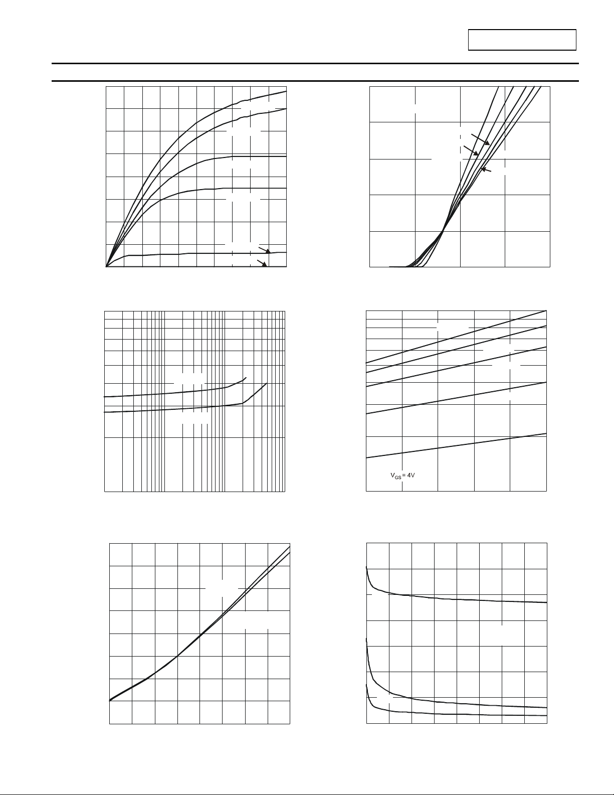
Fig. 1 Typical Output Characteri st ics
10
Ω
V= 2.5V
GS
V = 10V
GS
0.5
V = 10V
DS
(A)
AIN
D
I, D
0.4
0.3
0.2
T = 85°C
A
T = 25°C
A
T = -55°C
A
T = 150°C
A
T = 125°C
A
0.1
0
01 234
V , GATE SOURCE VOLTAGE (V)
GS
Fig. 2 Typical Transfer Characteristics
10
Ω
T = 150°C
A
E ( )
T = 125°C
A
T = 85°C
A
ESIS
T = 25°C
A
V = 4.0V
GS
T = -55°C
AIN-S
A
, D
DS(ON)
1
R , DRAIN-SOURCE ON-RESISTANCE ( )
0.001 0.01 0.1 1
I , DRAIN CURRENT (A)
D
Fig. 3 Typical On-Resistance
vs. Drain C urrent an d G at e Vol t age
2.0
1.8
V = 4V
1.6
1.4
1.2
GS
I = 100mA
D
V = 2.5V
GS
I = 80mA
D
1.0
0.8
DS(ON)
R , DRAIN-TO-SOURCE
RESISTANCE (NORMALIZED)
0.6
0.4
-50 -25 0 25 50 75 100 125 150
T , JUNCTION TEMPERATURE (°C)
J
Fig. 5 On- Resistance Variation with Temperature
DMB54D0UDW
Document number: DS31677 Rev. 4 - 2
3 of 7
www.diodes.com
DS(ON)
1
0 0.1 0.2 0.3 0.4 0.5
I , DRAIN CURRENT (A)
D
Fig. 4 Typical Drain-Source On-Resistance
vs. Drain Current and Tem peratur e
35
30
)
25
C
iss
E (p
20
I
15
A
f = 1MHz
V = 0V
GS
A
10
5
C
oss
C
rss
0
0 5 10 15 20 25 30 35 40
V , DRAIN-SOURCE VOLTAGE (V)
DS
Fig. 6 Typical Capacitance
December 2009
© Diodes Incorporated
 Loading...