Diodes DMB53D0UV User Manual

Y
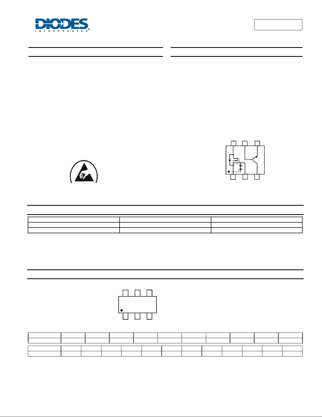
N-CHANNEL ENHANCEMENT MODE MOSFET PLUS NPN TRANSISTOR
Features
• N-Channel MOSFET and NPN Transistor in One Package
• Low On-Resistance
• Very Low Gate Threshold Voltage, 1.0V max
• Low Input Capacitance
• Fast Switching Speed
• Low Input/Output Leakage
• Ultra-Small Surface Mount Package
• ESD Protected MOSFET Gate up to 2kV
• Lead, Halogen and Antimony Free, RoHS Compliant (Note
• "Green" Device (Note 2)
• Qualified to AEC-Q101 Standards for High Reliability
ESD PROTECTED TO 2kV
Top View
1)
SOT563
DMB53D0UV
Mechanical Data
• Case: SOT563
• Case Material: Molded Plastic, “Green” Molding Compound.
UL Flammability Classification Rating 94V-0
• Moisture Sensitivity: Level 1 per J-STD-020
• Terminal Connections: See Diagram
• Terminals: Finish - Matte Tin annealed over Copper lead frame.
Solderable per MIL-STD-202, Method 208
• Weight: 0.006 grams (approximate)
D
Bottom View
2
Q
1
S
2
Top View
Internal Schematic
E
B
Q
2
G
C
2
Ordering Information (Note 3)
Part Number Case Packaging
DMB53D0UV-7 SOT563 3000/Tape & Reel
DMB53D0UV-13 SOT563 10000/Tape & Reel
Notes: 1. EU Directive 2002/95/EC (RoHS) & 2011/65/EU (RoHS 2) compliant. No purposely added lead. Halogen and Antimony free
2. Diodes Inc.’s “Green” policy can be found on our website at http://www.diodes.com.
3. For packaging details, go to our website at http://www.diodes.com.
Marking Information
MB1
M
Date Code Key
Year 2008 2009 2010 2011 2012 2013 2014 2015 2016 2017
Code V W X Y Z A B C D E
Month Jan Feb Mar Apr May Jun Jul Aug Sep Oct Nov Dec
Code 1 2 3 4 5 6 7 8 9 O N D
DMB53D0UV
Document number: DS31651 Rev. 7 - 2
www.diodes.com
MB1 = Marking Code
YM = Date Code Marking
Y = Year (ex: V = 2008)
M = Month (ex: 9 = September)
1 of 7
March 2012
© Diodes Incorporated

θ
)
Maximum Ratings – MOSFET, Q1 @T
= 25°C unless otherwise specified
A
Characteristic Symbol Value Units
Drain-Source Voltage
Gate-Source Voltage
Drain Current (Note 4) Continuous
Pulsed Drain Current (Note 4)
Maximum Ratings - NPN Transistor, Q2 @T
Characteristic Symbol Value Unit
Collector-Base Voltage
Collector-Emitter Voltage
Emitter-Base Voltage
Collector Current
V
DSS
V
GSS
I
D
I
DM
= 25°C unless otherwise specified
A
V
CBO
V
CEO
V
EBO
I
C
50 V
±12
160 mA
560 mA
50 V
45 V
6.0 V
100 mA
DMB53D0UV
V
Thermal Characteristics, Total Device @T
= 25°C unless otherwise specified
A
Characteristic Symbol Value Unit
Total Power Dissipation (Note 1)
Thermal Resistance, Junction to Ambient (Note 1)
Operating and Storage Temperature Range
P
D
R
JA
T
, T
J
STG
250 mW
500
-55 to +150
°C/W
°C
Electrical Characteristics - MOSFET @T
= 25°C unless otherwise specified
A
Characteristic Symbol Min Typ Max Unit Test Condition
OFF CHARACTERISTICS (Note 5)
Drain-Source Breakdown Voltage
Zero Gate Voltage Drain Current
Gate-Body Leakage
BV
I
DSS
I
GSS
DSS
50
⎯ ⎯
⎯ ⎯
⎯ ⎯
10
1.0
5.0
V
VGS = 0V, ID = 250μA
μA
V
= 50V, VGS = 0V
DS
= ±8V, V
V
μA
GS
= ±12V, V
V
GS
DS
DS
= 0V
= 0V
ON CHARACTERISTICS (Note 5)
Gate Threshold Voltage
Static Drain-Source On-Resistance
Forward Transconductance
V
GS(th
R
DS (ON)
g
FS
0.7 0.8 1.0 V
⎯
⎯
180
3.1 4
4 5
⎯ ⎯
VDS = VGS, ID = 250μA
V
= 4V, ID = 100mA
Ω
mS
GS
= 2.5V, ID = 80mA
V
GS
= 10V, ID = 100mA,
V
DS
f = 1.0KHz
DYNAMIC CHARACTERISTICS (Note 6)
Input Capacitance
Output Capacitance
Reverse Transfer Capacitance
Notes: 4. Device mounted on FR-4 substrate PC board, 2oz copper, with minimum recommended pad layout.
5. Short duration pulse test used to minimize self-heating effect.
6. Guaranteed by design. Not subject to product testing.
C
iss
C
oss
C
rss
DMB53D0UV
Document number: DS31651 Rev. 7 - 2
⎯
⎯
⎯
2 of 7
www.diodes.com
25
5
2.1
⎯
⎯
⎯
pF
pF
pF
V
= 10V, V
DS
f = 1.0MHz
= 0V,
GS
March 2012
© Diodes Incorporated

(BR)
(BR)
(BR)
R
CUR
RENT
R
CUR
RENT
Electrical Characteristics - NPN Transistor @T
= 25°C unless otherwise specified
A
Characteristic Symbol Min Typ Max Unit Test Condition
Collector-Base Breakdown Voltage (Note 5)
Collector-Emitter Breakdown Voltage (Note 5)
Emitter-Base Breakdown Voltage (Note 5)
DC Current Gain (Note 5)
Collector-Emitter Saturation Voltage (Note 5)
Base-Emitter Saturation Voltage (Note 5)
Base-Emitter Voltage (Note 5)
Collector-Cutoff Current (Note 5)
Collector-Emitter Cut-Off Current (Note 5)
Gain Bandwidth Product
Output Capacitance
V
V
V
h
V
CE(SAT)
V
BE(SAT)
V
I
CBO
I
CBO
I
CES
C
FE
BE
f
T
OBO
CBO
CEO
EBO
50 — — V
45 — — V
6 — — V
200 290 450 —
— —
—
580
—
— —
— — 100 nA
700
900
660
—
100
300
— mV
700
770
15
5.0
100 — — MHz
— — 4.5 pF
mV
mV
Noise Figure NF — — 10 dB
IC = 10μA, IB = 0
IC = 10mA, IB = 0
IE = 1μA, IC = 0
VCE = 5.0V, IC = 2.0mA
= 10mA, IB = 0.5mA
I
C
= 100mA, IB = 5.0mA
I
C
I
= 10mA, IB = 0.5mA
C
I
= 100mA, IB = 5.0mA
C
= 5.0V, IC = 2.0mA
V
CE
V
= 5.0V, IC = 10mA
CE
V
nA
µA
= 30V
CB
= 30V, TA = 150°C
V
CB
VCE = 45V
V
= 5.0V, IC = 10mA,
CE
f = 100MHz
VCB = 10V, f = 1.0MHz
V
= 5V, RS = 2.0kΩ,
CE
f = 1.0kHz, BW = 200Hz
DMB53D0UV
MOSFET
0.8
V = 10V
0.7
0.6
GS
V = 4.5V
GS
(A)
0.5
V = 3.0V
GS
0.4
V = 2.5V
AIN
D
I, D
0.3
0.2
0.1
0
GS
V = 1.5V
GS
V = 1.0V
GS
0 0.5 1 1.5 2 2.5 3 3.5 4 4.5 5
V , DRAIN-SOURCE VOLTAGE (V)
DS
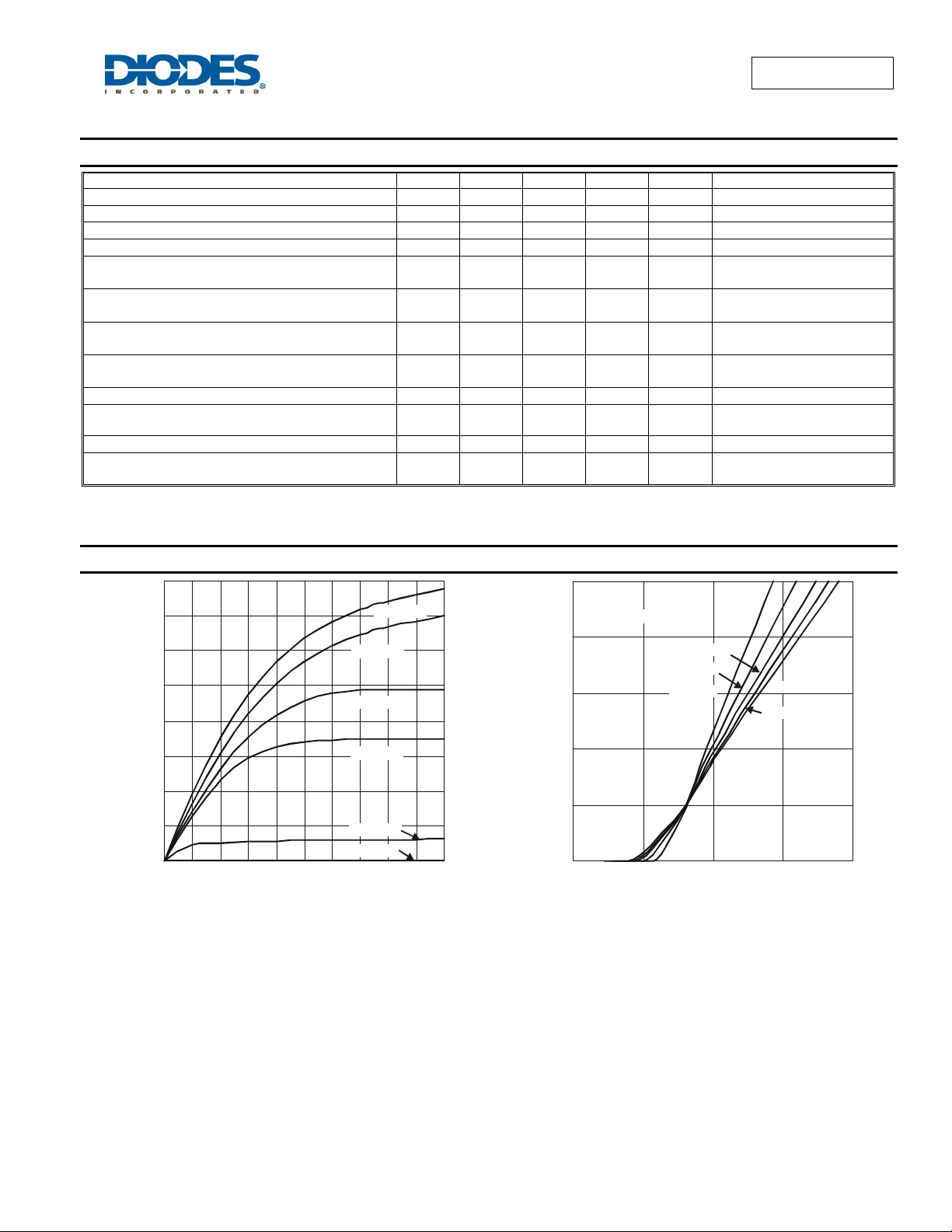
Fig. 1 Typical Output Characteristics
DMB53D0UV
Document number: DS31651 Rev. 7 - 2
3 of 7
www.diodes.com
0.5
V = 10V
DS
(A)
AIN
D
I, D
0.4
0.3
0.2
T = 85°C
A
T = 25°C
A
T = -55°C
A
T = 150°C
A
T = 125°C
A
0.1
0
01 234
V , GATE SOURCE VOLTAGE (V)
GS
Fig. 2 Typical Transfer Characteristics
March 2012
© Diodes Incorporated
 Loading...