

Page 1
θ
Please click here to visit our online spice models database.
N-CHANNEL ENHANCEMENT MODE MOSFET PLUS NPN TRANSISTOR
Features
• N-Channel MOSFET and NPN Transistor in One Package
• Low On-Resistance
• Very Low Gate Threshold Voltage, 1.0V max
• Low Input Capacitance
• Fast Switching Speed
• Low Input/Output Leakage
• Ultra-Small Surface Mount Package
• Lead, Halogen and Antimony Free, RoHS Compliant (Note
• ESD Protected MOSFET Gate up to 2kV
• "Green" Device (Note 3)
• Qualified to AEC-Q101 Standards for High Reliability
ESD protected gate up to 2kV
2)
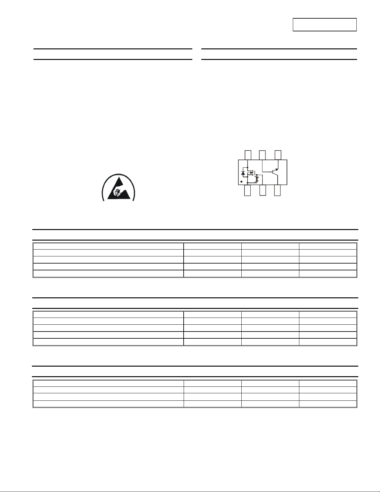
SOT-363
TOP VIEW
DMB53D0UDW
Mechanical Data
• Case: SOT-363
• Case Material: Molded Plastic, “Green” Molding Compound.
UL Flammability Classification Rating 94V-0
• Moisture Sensitivity: Level 1 per J-STD-020
• Terminal Connections: See Diagram
• Terminals: Finish - Matte Tin annealed over Alloy 42 Lead frame.
Solderable per MIL-STD-202, Method 208
• Marking Information: See Page 5
• Ordering Information: See Page 5
• Weight: 0.006 grams (approximate)
D
2
Q
1
S
2
TOP VIEW
Internal Schematic
E
B
Q
2
G
C
2
Maximum Ratings – MOSFET, Q1 @T
Characteristic Symbol Value Units
Drain-Source Voltage
Gate-Source Voltage
Drain Current (Note 1) Continuous
Pulsed Drain Current (Note 1)
Maximum Ratings - NPN Transistor, Q2 @T
Characteristic Symbol Value Unit
Collector-Base Voltage
Collector-Emitter Voltage
Emitter-Base Voltage
Collector Current
Thermal Characteristics, Total Device @T
Characteristic Symbol Value Unit
Total Power Dissipation (Note 1)
Thermal Resistance, Junction to Ambient (Note 1)
Operating and Storage Temperature Range
Notes: 1. Device mounted on FR-4 PCB, 1 inch x 0.85 inch x 0.062 inch; pad layout as shown on Diodes Inc. suggested pad layout document AP02001, which
3. Diodes Inc.’s “Green” policy can be found on our website at http://www.diodes.com/products/lead_free/index.php.
DMB53D0UDW
Document number: DS31675 Rev. 5 - 2
can be found on our website at http://www.diodes.com/datasheets/ap02001.pdf.
2. No purposefully added lead. Halogen and Antimony Free.
= 25°C unless otherwise specified
A
V
DSS
V
GSS
I
D
I
DM
= 25°C unless otherwise specified
A
V
CBO
V
CEO
V
EBO
I
C
= 25°C unless otherwise specified
A
P
D
R
JA
T
, T
J
STG
1 of 7
www.diodes.com
50 V
±12
V
160 mA
560 mA
50 V
45 V
6.0 V
100 mA
250 mW
500
-55 to +150
°C/W
°C
December 2009
© Diodes Incorporated
Page 2

)
(BR)
(BR)
(BR)
Electrical Characteristics - MOSFET @T
= 25°C unless otherwise specified
A
Characteristic Symbol Min Typ Max Unit Test Condition
OFF CHARACTERISTICS (Note 2)
Drain-Source Breakdown Voltage
Zero Gate Voltage Drain Current
Gate-Body Leakage
BV
I
DSS
I
GSS
DSS
50
⎯ ⎯
⎯ ⎯
⎯ ⎯
10
1.0
5.0
ON CHARACTERISTICS (Note 2)
Gate Threshold Voltage
Static Drain-Source On-Resistance
Forward Transconductance
V
GS(th
R
DS (ON)
g
FS
0.7 0.8 1.0 V
⎯
⎯
180
3.1 4
4 5
⎯ ⎯
mS
DYNAMIC CHARACTERISTICS
Input Capacitance
Output Capacitance
Reverse Transfer Capacitance
C
⎯
iss
C
⎯
oss
C
⎯
rss
Electrical Characteristics - NPN Transistor @T
= 25°C unless otherwise specified
A
25
5
2.1
⎯
⎯
⎯
Characteristic Symbol Min Typ Max Unit Test Condition
Collector-Base Breakdown Voltage (Note 4)
Collector-Emitter Breakdown Voltage (Note 4)
Emitter-Base Breakdown Voltage (Note 4)
DC Current Gain (Note 4)
Collector-Emitter Saturation Voltage (Note 4)
Base-Emitter Saturation Voltage (Note 4)
Base-Emitter Voltage (Note 4)
Collector Cut-Off Current (Note 4)
Collector-Emitter Cut-Off Current (Note 4)
Gain Bandwidth Product
Output Capacitance
V
V
V
h
V
CE(SAT)
V
BE(SAT)
V
I
CBO
I
CES
C
FE
BE
f
T
OBO
CBO
CEO
EBO
50 — — V
45 — — V
6 — — V
200 290 450 —
— —
—
580
—
— —
— — 100 nA
700
900
660
—
100
300
— mV
700
770
15
5.0
100 — — MHz
— — 4.5 pF
mV
mV
Noise Figure NF — — 10 dB
Notes: 4. Short duration pulse test used to minimize self-heating effect.
DMB53D0UDW
V
VGS = 0V, ID = 250μA
μA
V
= 50V, VGS = 0V
DS
= ±8V, V
V
μA
Ω
pF
pF
pF
nA
µA
GS
V
= ±12V, V
GS
VDS = VGS, ID = 250μA
= 4V, ID = 100mA
V
GS
VGS = 2.5V, ID = 80mA
V
= 10V, ID = 100mA,
DS
f = 1.0KHz
= 10V, V
V
DS
f = 1.0MHz
IC = 10μA, IB = 0
IC = 10mA, IB = 0
IE = 1μA, IC = 0
VCE = 5.0V, IC = 2.0mA
= 10mA, IB = 0.5mA
I
C
= 100mA, IB = 5.0mA
I
C
I
= 10mA, IB = 0.5mA
C
I
= 100mA, IB = 5.0mA
C
= 5.0V, IC = 2.0mA
V
CE
V
= 5.0V, IC = 10mA
CE
= 30V
V
CB
= 30V, TA = 150°C
V
CB
VCE = 45V
V
= 5.0V, IC = 10mA,
CE
f = 100MHz
VCB = 10V, f = 1.0MHz
V
= 5V, RS = 2.0kΩ,
CE
f = 1.0kHz, BW = 200Hz
DS
GS
= 0V
DS
= 0V,
= 0V
DMB53D0UDW
Document number: DS31675 Rev. 5 - 2
2 of 7
www.diodes.com
December 2009
© Diodes Incorporated
Page 3
R
C
URRENT
R
CUR
RENT
R
R
OUR
CE ON-R
TANC
C, C
P
C
TAN
C
F
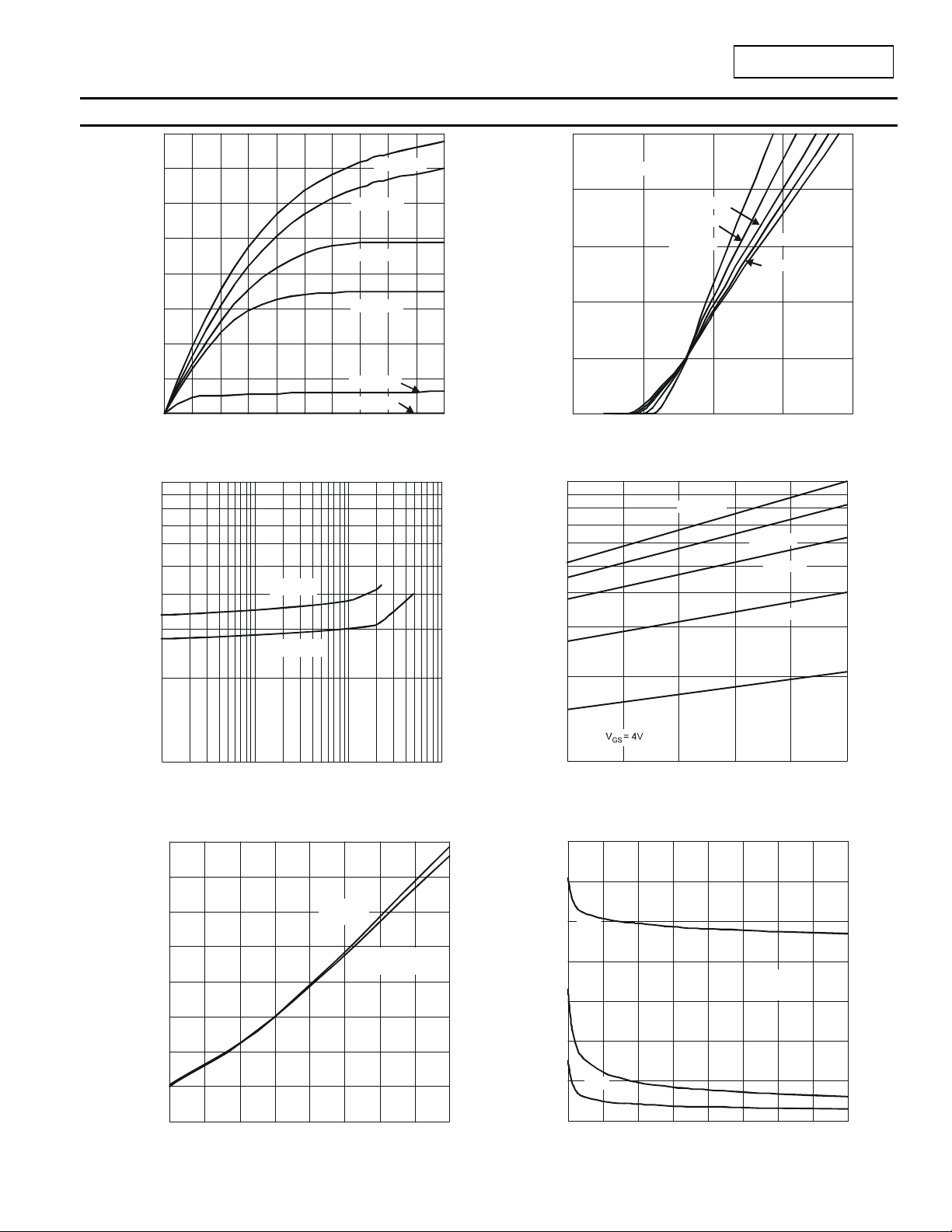
DMB53D0UDW
MOSFET
0.8
0.7
0.6
V = 4.5V
GS
(A)
0.5
V = 3.0V
GS
0.4
V = 2.5V
AIN
D
I, D
0.3
0.2
0.1
0
GS
V = 1.5V
GS
V = 1.0V
GS
0 0.5 1 1.5 2 2.5 3 3.5 4 4.5 5
V , DRAIN-SOURCE VOLTAGE (V)
DS
Fig. 1 Typical Output Characteri st ics
10
Ω
V= 2.5V
GS
V = 10V
GS
0.5
V = 10V
DS
(A)
AIN
D
I, D
0.4
0.3
0.2
T = 85°C
A
T = 25°C
A
T = -55°C
A
T = 150°C
A
T = 125°C
A
0.1
0
01 234
V , GATE SOURCE VOLTAGE (V)
GS
Fig. 2 Typical Transfer Characteristics
10
Ω
T = 150°C
A
E ( )
T = 125°C
A
T = 85°C
A
ESIS
T = 25°C
A
V = 4.0V
GS
T = -55°C
AIN-S
A
, D
DS(ON)
1
R , DRAIN-SOURCE ON-RESISTANCE ( )
0.001 0.01 0.1 1
I , DRAIN CURRENT (A)
D
Fig. 3 Typical On-Resistance
vs. Drain C urrent an d G at e Vol t age
2.0
1.8
V = 4V
1.6
1.4
1.2
GS
I = 100mA
D
V = 2.5V
GS
I = 80mA
D
1.0
0.8
DS(ON)
R , DRAIN-TO-SOURCE
RESISTANCE (NORMALIZED)
0.6
0.4
-50 -25 0 25 50 75 100 125 150
T , JUNCTION TEMPERATURE (°C)
J
Fig. 5 On- Resistance Variation with Temperature
DMB53D0UDW
Document number: DS31675 Rev. 5 - 2
3 of 7
www.diodes.com
DS(ON)
1
0 0.1 0.2 0.3 0.4 0.5
I , DRAIN CURRENT (A)
D
Fig. 4 Typical Drain-Source On-Resistance
vs. Drain Current and Temperature
35
30
)
25
C
iss
E (p
20
I
15
A
f = 1MHz
V = 0V
GS
A
10
5
C
oss
C
rss
0
0 5 10 15 20 25 30 35 40
V , DRAIN-SOURCE VOLTAGE (V)
DS
Fig. 6 Typical Capacitance
December 2009
© Diodes Incorporated
Page 4

OUR
CE CUR
RENT
P, P
OWER
PATIO
N
DMB53D0UDW
MOSFET (continued)
1.1
1.0
0.9
0.8
0.7
0.6
GS(TH)
V , GATE THRESHOLD VOLTAGE (V)
0.5
-50 -25 0 25 50 75 100 125 150
Fig. 7 Gat e Threshol d Variation vs. Ambien t Temperature
300
T , AMBIENT TEMPERATURE (°C)
A
I = 250µA
D
1
0.1
(A)
T = 150°C
A
T = 125°C
0.01
0.001
S
I, S
0.0001
A
T = 85°C
A
T = 25°C
A
0.1 0.3 0.5 0.7 0.9 1.1
V , SOURCE-DRAIN VOLTAGE (V)
SD
Fig. 8 Diode Forwar d Vol t age vs. Cu r re nt
T = -55°C
A
250
(mW)
200
150
DISSI
100
D
50
RC/W
°
= 500
θ
JA
0
-50 0
T , AMBIENT TEMPERATURE ( C)
Fig. 9 Derating Curve - Total Package Power Dissipation
A
50
100 150
°
DMB53D0UDW
Document number: DS31675 Rev. 5 - 2
4 of 7
www.diodes.com
December 2009
© Diodes Incorporated
Page 5

C C
URREN
T GAIN
C
O
CTO
R
T
TER
GAIN
N
T
H PRODUCT
H
DMB53D0UDW
NPN Transistor
1,000
T = 150 C
A
°
T = 25C
A
100
10
FE,
h D
T = -50C
°
A
1
1
10
I , COLLECTOR CURRENT (mA)
C
100 1,000
Fig. 10 Typical DC Current Gain vs. Collector Current
1,000
V = 5V
z)
CE
°
0.3
-EMI
LLE
SATURATION VOLTAGE (V)
CE(SAT)
V,
0.4
I
C
= 20
I
B
0.2
T = 150°C
A
T = 25°C
A
0.1
T = -50°C
A
0
10.1 10
I , COLLECTOR CURRENT (mA)
C
100
Fig. 11 T ypical Collector-Emitter Saturation Voltage
vs. Collector Current
1,000
(M
100
DWID
10
-BA
T
f,
1
110100
I , COLLECTOR CURRENT (mA)
C
Fig. 12 Typical Gain-Bandwidth Product
vs. Collector Current
Ordering Information (Note 5)
Part Number Case Packaging
DMB53D0UDW-7 SOT-363 3000/Tape & Reel
Notes: 5. For packaging details, go to our website at http://www.diodes.com/datasheets/ap02007.pdf.
Marking Information
M1B
YM
Date Code Key
Year 2008 2009 2010 2011 2012 2013 2014 2015
Code V W X Y Z A B C
Month Jan Feb Mar Apr May Jun Jul Aug Sep Oct Nov Dec
Code 1 2 3 4 5 6 7 8 9 O N D
DMB53D0UDW
Document number: DS31675 Rev. 5 - 2
www.diodes.com
MB1 = Marking Code
YM = Date Code Marking
Y = Year (ex: V = 2008)
M = Month (ex: 9 = September)
5 of 7
December 2009
© Diodes Incorporated
Page 6

Package Outline Dimensions
A
K
J
H
D
F
Suggested Pad Layout
G
Z
Y
X
B C
C2
DMB53D0UDW
SOT-363
Dim Min Max
A 0.10 0.30
B 1.15 1.35
C 2.00 2.20
D 0.65 Typ
F 0.40 0.45
H 1.80 2.20
M
L
C2
C1
J 0 0.10
K 0.90 1.00
L 0.25 0.40
M 0.10 0.22
0° 8°
α
All Dimensions in mm
Dimensions Value (in mm)
Z 2.5
G 1.3
X 0.42
Y 0.6
C1 1.9
C2 0.65
DMB53D0UDW
Document number: DS31675 Rev. 5 - 2
6 of 7
www.diodes.com
December 2009
© Diodes Incorporated
Page 7

IMPORTANT NOTICE
DIODES INCORPORATED MAKES NO WARRANTY OF ANY KIND, EXPRESS OR IMPLIED, WITH REGARDS TO THIS DOCUMENT,
INCLUDING, BUT NOT LIMITED TO, THE IMPLIED WARRANTIES OF MERCHANTABILITY AND FITNESS FOR A PARTICULAR PURPOSE
(AND THEIR EQUIVALENTS UNDER THE LAWS OF ANY JURISDICTION).
Diodes Incorporated and its subsidiaries reserve the right to make modifications, enhancements, improvements, corrections or other changes
without further notice to this document and any product described herein. Diodes Incorporated does not assume any liability arising out of the
application or use of this document or any product described herein; neither does Diodes Incorporated convey any license under its patent or
trademark rights, nor the rights of others. Any Customer or user of this document or products described herein in such applications shall assume
all risks of such use and will agree to hold Diodes Incorporated and all the companies whose products are represented on Diodes Incorporated
website, harmless against all damages.
Diodes Incorporated does not warrant or accept any liability whatsoever in respect of any products purchased through unauthorized sales channel.
Should Customers purchase or use Diodes Incorporated products for any unintended or unauthorize d application, Customers shall indemnify and
hold Diodes Incorporated and its representatives harmless against all claims, damages, expenses, and attorney fees arising out of, directly or
indirectly, any claim of personal injury or death associated with such unintended or unauthorized application.
Products described herein may be covered by one or more United States, international or foreign patents pending. Product names and markings
noted herein may also be covered by one or more United States, international or foreign trademarks.
LIFE SUPPORT
Diodes Incorporated products are specifically not authorized for use as critical components in life support devices or systems without the express
written approval of the Chief Executive Officer of Diodes Incorporated. As used herein:
A. Life support devices or systems are devices or systems which:
1. are intended to implant into the body, or
2. support or sustain life and whose failure to perform when properly used in accordance with instructions for use provided in the
labeling can be reasonably expected to result in significant injury to the user.
B. A critical component is any component in a life support device or system whose failure to perform can be reasonably expected to cause the
failure of the life support device or to affect its safety or effectiveness.
Customers represent that they have all necessary expertise in the safety and regulatory ramifications of their life support devices or systems, and
acknowledge and agree that they are solely responsible for all legal, regulatory and safety-related requirements concerning their products and any
use of Diodes Incorporated products in such safety-critical, life support devices or systems, notwithstanding any devices- or systems-related
information or support that may be provided by Diodes Incorporated. Further, Customers must fully indemnify Diodes Incorporated and its
representatives against any damages arising out of the use of Diodes Incorporated products in such safety-critical, life support devices or systems.
Copyright © 2009, Diodes Incorporated
www.diodes.com
DMB53D0UDW
DMB53D0UDW
Document number: DS31675 Rev. 5 - 2
7 of 7
www.diodes.com
December 2009
© Diodes Incorporated
 Loading...