

Page 1
yp
Features
• Complementary Pair
• Epitaxial Planar Die Construction
• One 22
22A Type (NPN),
One 2907A Type (PNP)
• Ideal for Lo
• Lead Free
• "Gree
w Power Amplification and Switching
By Design/RoHS Compliant (Note 2)
n Device" (Note 3)
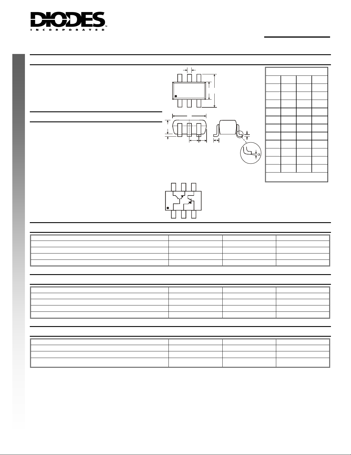
Mechanical Data
• Case: SOT-26
• Case Material: M
Compound. UL Flammability Classification Rating 94V-0
• Moisture Sensitivity
• Terminals: Finish - Matte Tin a
leadframe. Solderable per MIL-STD-202, Method 208
• Terminal Conn
• Orde
NEW PRODUCT
• Marking Informat
ring & Date Code Information: See Page 6
• Weight: 0.006 gr
olded Plastic, “Green” Molding
ections: See Diagram
ion: See Page 6
ams (approximate)
COMPLEMENTARY NPN / PNP SMALL SIGNAL SURFACE MOUNT TRANSISTOR
: Level 1 per J-STD-020C
nnealed over Copper
A
K
J
E
C
1
1
E2B
B
1
H
D
C
2
C
B
2
M
L
F
Note: E1, B1, and C1 = 2222A Type (NPN)
E2, B2, and C2 = 2907A Type (PNP)
T
e marking indicates orientation
C
E
C
1
2
1
DMB2227A
SOT-26
Dim Min Max Typ
A 0.35 0.50 0.38
B 1.50 1.70 1.60
C 2.70 3.00 2.80
D – – 0.95
F – – 0.55
H 2.90 3.10 3.00
J 0.013 0.10 0.05
K 1.00 1.30 1.10
L 0.35 0.55 0.40
M 0.10 0.20 0.15
0° 8°
α
All Dimensi mm ons in
–
Maximum Ratings: 2222A Type (NPN) @T
Characteristic Symbol 2222A (NPN) Unit
Collector-Base Voltage
Collector-Emitter Voltage
Emitter-Base Voltage
Collector Current - Continuous
Maximum Ratings: 2907A Type (PNP) @T
Characteristic Symbol 2907A (PNP) Unit
Collector-Base Voltage
Collector-Emitter Voltage
Emitter-Base Voltage
Collector Current - Continuous
Maximum Ratings: Total @T
Characteristic Symbol Value Unit
Power Dissipation (Note 1)
Thermal Resistance, Junction to Ambient (Note 1)
Operating and Storage Temperature Range
Notes: 1. Device mounted on FR-4 PCB, 1 inch x 0.85 inch x 0.062 inch; pad layout as shown on Diodes Inc. suggested pad layout document AP02001, which
DS31217 Rev. 4 - 2 1 of 6
can be found on our website at http://www.diodes.com/datasheets/ap02001.pdf.
2. No purposefully added lead.
3. Diodes Inc.'s "Green" policy can be found on our website at http://www.diodes.com/products/lead_free/index.php.
= 25°C unless otherwise specified
A
B
2E2B1
= 25°C unless otherwise specified
A
V
CBO
V
CEO
V
EBO
I
C
= 25°C unless otherwise specified
A
V
CBO
V
CEO
V
EBO
I
C
P
D
R
JA
θ
T
, T
j
STG
www
.diodes.com
75 V
40 V
6.0 V
600 mA
-60 V
-60 V
-5.0 V
-600 mA
300 mW
417
-55 to +150
°C/W
°C
DMB2227A
© Diodes Incorporated
Page 2
Electrical Characteristics: 2222A Type (NPN) @T
OFF CHARACTERISTICS (Note 4)
Collector-Base Breakdown Voltage
Collector-Emitter Breakdown Voltage
Emitter-Base Breakdown Voltage
Collector Cutoff Current
Collector Cutoff Current
Emitter Cutoff Current
Base Cutoff Current
ON CHARACTERISTICS (Note 4)
DC Current Gain
Collector-Emitter Saturation Voltage
NEW PRODUCT
Base-Emitter Saturation Voltage
SMALL SIGNAL CHARACTERISTICS
Output Capacitance
Input Capacitance
Current Gain-Bandwidth Product
SWITCHING CHARACTERISTICS
Delay Time
Rise Time
Storage Time
Fall Time
Notes: 4. Pulse test: pulse width ≤300μS, duty cycle ≤2%.
DS31217 Rev. 4 - 2 2 of 6
Characteristic Symbol Min Max Unit Test Condition
www.diodes.com
V
(BR)CBO
V
(BR)CEO
V
(BR)EBO
I
CBO
I
CEX
I
EBO
I
h
V
CE(SAT)
V
BE(SAT)
C
C
BL
FE
obo
ibo
f
T
t
d
t
t
t
= 25°C unless otherwise specified
A
75
40
6.0
⎯
⎯
⎯
⎯
35
50
75
100
40
50
35
⎯
0.6
⎯
⎯
⎯
⎯
⎯
10
10 nA
10 nA
20 nA
⎯
⎯
⎯
300
⎯
⎯
⎯
0.3
1.0
1.2
2.0
8 pF
— 25 pF
300
⎯
r
s
f
⎯
⎯
⎯
⎯
10 ns
25 ns
225 ns
60 ns
V
I
= 10μA, IE = 0
C
V
I
= 10mA, IB = 0
C
V
I
= 10μA, IC = 0
E
nA
μA
⎯
V
V
= 60V, IE = 0
V
CB
V
= 60V, IE = 0, TA = 150°C
CB
V
= 60V, V
CE
V
= 3.0V, IC = 0
EB
V
= 60V, V
CE
= 100μA, V
I
C
= 1.0mA, VCE = 10V
I
C
I
= 10mA, VCE = 10V
C
= 150mA, V
I
C
I
= 500mA, VCE = 10V
C
= 10mA, VCE = 10V, TA = -55°C
I
C
I
= 150mA, VCE = 1.0V
C
= 150mA, IB = 15mA
I
C
= 500mA, IB = 50mA
I
C
= 150mA, IB = 15mA
I
C
= 500mA, IB = 50mA
I
C
VCB = 10V, f = 1.0MHz, IE = 0
V
= 0.5V, f = 1.0MHz, IC = 0
EB
= 20V, IC = 20mA,
V
MHz
CE
f = 100MHz
V
= 30V, IC = 150mA,
CC
V
= - 0.5V, IB1 = 15mA
BE(off)
V
= 30V, IC = 150mA,
CC
= IB2 = 15mA
I
B1
EB(OFF)
EB(OFF)
= 10V
CE
= 10V
CE
= 3.0V
= 3.0V
DMB2227A
© Diodes Incorporated
Page 3

P, P
O
R
PATIO
Electrical Characteristics: 2907A Type (PNP) @T
OFF CHARACTERISTICS (Note 4)
Collector-Base Breakdown Voltage
Collector-Emitter Breakdown Voltage
Emitter-Base Breakdown Voltage
Collector Cutoff Current
Collector Cutoff Current
Base Cutoff Current
ON CHARACTERISTICS (Note 4)
DC Current Gain
Collector-Emitter Saturation Voltage
Base-Emitter Saturation Voltage
SMALL SIGNAL CHARACTERISTICS
NEW PRODUCT
Output Capacitance
Input Capacitance
Current Gain-Bandwidth Product
SWITCHING CHARACTERISTICS
Turn-On Time
Delay Time
Rise Time
Turn-Off Time
Storage Time
Fall Time
400
Characteristic Symbol Min Max Unit Test Condition
V
(BR)CBO
V
(BR)CEO
V
(BR)EBO
I
CBO
I
CEX
I
BL
h
FE
V
CE(SAT)
V
BE(SAT)
C
obo
C
ibo
f
T
t
on
t
d
t
r
t
off
t
s
t
f
= 25°C unless otherwise specified
A
-60
-60
-5.0
⎯
⎯
⎯
75
100
100
100
50
⎯
⎯
⎯
⎯
⎯
⎯
-10
-50 nA
-50 nA
⎯
⎯
⎯
300
⎯
-0.4
-1.6
-1.3
-2.6
8.0 pF
V
V
V
nA
μA
⎯
V
V
— 30 pF
200
⎯
⎯
⎯
⎯
⎯
⎯
⎯
45 ns
10 ns
40 ns
100 ns
80 ns
30 ns
MHz
I
= -10μA, IE = 0
C
I
= -10mA, IB = 0
C
I
= -10μA, IC = 0
E
= -50V, IE = 0
V
CB
V
= -50V, IE = 0, TA = 125°C
CB
V
= -30V, V
CE
V
= -30V, V
CE
I
= -100µA, V
C
= -1.0mA, VCE = -10V
I
C
I
= -10mA, VCE = -10V
C
= -150mA, V
I
C
I
= -500mA, VCE = -10V
C
= -150mA, IB = -15mA
I
C
= -500mA, IB = -50mA
I
C
= 150mA, IB = 15mA
I
C
= 500mA, IB = 50mA
I
C
EB(OFF)
EB(OFF)
= -10V
CE
= -10V
CE
= -0.5V
= -0.5V
VCB = -10V, f = 1.0MHz, IE = 0
V
= -2.0V, f = 1.0MHz, IC = 0
EB
V
= -20V, IC = -50mA, f = 100MHz
CE
= -30V, IC = -150mA,
V
CC
= -15mA
I
B1
= -6.0V, IC = -150mA,
V
CC
I
= IB2 = -15mA
B1
350
300
N (mW)
250
200
DISSI
150
WE
100
D
50
0
0
25 50
T , AMBIENT TEMPERATURE (°C)
A
75
100 125
150
175
200
Fig. 1, Max Power Dissipation vs.
Ambie nt Temper at ure
DS31217 Rev. 4 - 2 3 of 6
www
.diodes.com
DMB2227A
© Diodes Incorporated
Page 4

SATURATION VOLT AGE (V)
CE(SAT)
V , COLLECTOR EMITTER
I , COLLECTOR CURRENT (mA)
C
NEW PRODUCT
BE(ON)
V , BASE EMITTER TURN-ON VOLTAGE (V)
I , COLLECTOR CURRENT (mA)
C
BE(SAT)
V , BASE EMITTER SATURATION VOLTAGE (V)
I , COLLECTOR CURRENT (mA)
C
CAPACITANCE (pF)
V , REVERSE VOLTAGE (V)
R
DS31217 Rev. 4 - 2 4 of 6
.diodes.com
www
V = 20V
CE
f = 100MHz
Fig. 7 Typical Gain-Bandwidth Product
vs. Collector Current (2222A)
© Diodes Incorporated
DMB2227A
Page 5

T
TER TURN-O
OLTAG
NEW PRODUCT
CAP
C
TANC
F
G
T
H P
R
ODU
C
T
H
FE
h , DC CURRENT GAIN
-I , COLLECTOR CURRENT (A)
Fig. 8 Typical DC Current Gain vs. Collector Current (2907A)
1.2
E (V)
1
C
SATURA TION VO LTAGE (V)
CE(SAT)
-V , COLLECTOR-EMITTER
-I , COLLECTOR CURRENT (mA)
C
Fig. 9 Typical Collector-Emitter Saturation Voltage
vs. Collector Current (2907A)
1.2
I/I = 10
CB
1
N V
0.8
0.6
0.4
0.2
BE(ON)
0
-V , BASE-EMI
0.1 100
110
-I , COLLECTOR CURRENT (mA)
C
Fig. 10 Typical Base-Emitter Turn-On Voltage
vs. Collector Current (2907A)
35
30
25
)
E (p
20
I
15
A
1,000
0.8
0.6
0.4
BE(SAT)
-V , BASE-EMITTER
SATURATION VOLTAGE (V)
0.2
0
0.1
1
-I , COLLECTOR CURRENT (mA)
C
10
100
1,000
Fig. 11 T ypical Base-Emitter Saturation Voltage
vs. Collector Current (2907A)
500
450
z)
400
(M
350
300
250
200
10
5
0
0.1
110
V , REVERSE VOLTAGE (V)
R
Fig. 12 Typical Capacitance Characteristics (2907A)
100
DS31217 Rev. 4 - 2 5 of 6
.diodes.com
www
150
100
AIN BANDWID
T
f,
50
0
040
20
-I , COLLECTOR CURRENT (mA)
C
Fig. 13 Typical Gain-B andwidth Product
vs. Collector Current (2907A)
60
80
100
DMB2227A
© Diodes Incorporated
Page 6

Ordering Information (Note 5)
Device
DMB2227A-7
Notes: 5. For packaging details, go to our website at http://www.diodes.com/datasheets/ap02007.pdf.
Packaging Shipping
SOT-26 3000/Tape & Reel
Marking Information
Date Code Key
Year 2007 2008 2009 2010 2011 2012
Code U V W X Y Z
Month Jan Feb Mar Apr May Jun Jul Aug Sep Oct Nov Dec
Code 1 2 3 4 5 6 7 8 9 O N D
NEW PRODUCT
Diodes Incorporated and its subsidiaries reserve the right to make modifications, enhancements, improvements, corrections or other changes
without further notice to any product herein. Diodes Incorporated does not assume any liability arising out of the application or use of any product
described herein; neither does it convey any license under its patent rights, nor the rights of others. The user of products in such applications shall
assume all risks of such use and will agree to hold Diodes Incorporated and all the companies whose products are represented on our website,
harmless against all damages.
Diodes Incorporated products are not authorized for use as critical components in life support devices or systems without the expressed written
approval of the President of Diodes Incorporated.
D27
D27 = Product Type Marking Code
M = Date Code Marking
Y
Y = Year ex: U = 2007
YM
M = Month ex: 9 = September
IMPORTANT NOTICE
LIFE SUPPORT
DS31217 Rev. 4 - 2 6 of 6
www.diodes.com
DMB2227A
© Diodes Incorporated
 Loading...