

Page 1
A
Features
• 300 Watts Peak Pulse Power (tp = 8x20µs)
• Transient Protection for Data Line to IEC61000-4-2 level 4 (ESD),
8kV HBM
Contact: Discharge ±30kV
Air: Discharge ±30kV
• IEC 61000-4-4 (EFT)
• Low Leakage Current
• Surface Mount Package Ideally Suited for Automated Insertion
• Totally Lead-Free & Fully RoHS Compliant (Notes 1 & 2)
• Halogen and Antimony Free. “Green” Device (Note 3)
NEW PRODUCT
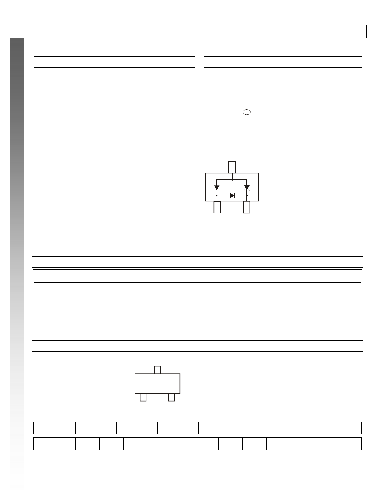
SOT323
Top View Device Schematic
DLPT05W
SURFACE MOUNT DATALINE PROTECTION DEVICE
Mechanical Data
• Case: SOT323
• Case Material: Molded Plastic. UL Flammability Classification
Rating 94V-0
• Moisture Sensitivity: Level 1 per J-STD-020
• Terminals: Solderable per MIL-STD-202, Method 208
• Lead Free Plating (Matte Tin Finish annealed over Alloy 42
leadframe)
• Terminal Connections: See Diagram
• Weight: 0.006 grams (approximate)
GROUND
LINE TO
BE PROTECTED
e3
V
TVS
CC
Ordering Information (Note 4)
Part Number Case Packaging
DLPT05W-7 SOT323 3000/Tape & Reel
Notes: 1. No purposely added lead. Fully EU Directive 2002/95/EC (RoHS) & 2011/65/EU (RoHS 2) compliant.
2. See http://www.diodes.com for more information about Diodes Incorporated’s definitions of Halogen- and Antimony-free, "Green" and Lead-free.
3. Halogen- and Antimony-free "Green” products are defined as those which contain <900ppm bromine, <900ppm chlorine (<1500ppm total Br + Cl) and
<1000ppm antimony compounds.
4. For packaging details, go to our website at http://www.diodes.com.
Marking Information
Date Code Key
Year 2011 2012 2013 2014 2015 2016 2017
Code Y Z A B C D E
Month Jan Feb Mar Apr May Jun Jul Aug Sep Oct Nov Dec
Code 1 2 3 4 5 6 7 8 9 O N D
AT1
YM
DLPT05W
Document number: DS35592 Rev. 3 - 2
T1 = Product Type Marking Code
YM = Date Code Marking
Y = Year (ex: Z = 2012)
M = Month (ex: 9 = September)
1 of 5
www.diodes.com
June 2012
© Diodes Incorporated
Page 2
θ
P
P
U
R
T
G
O
DLPT05W
Maximum Ratings @T
= 25°C unless otherwise specified
A
Characteristic Symbol Value Unit
Peak Pulse Power (tp = 8x20µs, per Figure 2 )
Peak Forward Voltage (I
= 1A, tp = 8x20µs, per Figure 2) VFP
PP
Diode Peak Repetitive Reverse Voltage
V
P
RRM
PK
300 W
2.1 V
75 V
Thermal Characteristics
Characteristic Symbol Value Unit
Thermal Resistance, Junction to Ambient (Note 5)
Operating and Storage Temperature Range
R
JA
T
, T
J
STG
NEW PRODUCT
Electrical Characteristics @T
Reverse
Standoff
Voltage
V
RWM
Notes: 5. Device mounted on FR-4 PCB pad layout (2oz copper) as shown on Diodes, Inc. suggested pad layout AP02001, which can be found on our website at
Breakdown Voltage
@ IT
V
BR
Min (V) Max (V)
(V)
5 6.0
http://www.diodes.com.
6. Short duration pulse test used to minimize self-heating effect.
7. Clamping voltage value is based on an 8x20μs peak pulse current (I
8. Measured from line to be protected to ground pin.
9. V
= 0V, f = 1MHz from line to be protected to ground pin.
R
⎯
= 25°C unless otherwise specified
A
Test
Current
Max. Reverse
Leakage @ V
(Note 6)
RWM
Max. Clamping
Voltage @ I
(Notes 7 & 8)
pp
= 1A
IT (mA) IR (μA) VC (V)
1.0 20 9.8 17 1.9
) waveform.
pp
100
625
-55 to +150
Max. Peak Pulse
Current
(Notes 7 & 8)
pp(A) (pF)
I
°C/W
Typical Total
Capacitance
°C
(Note 9)
F
75
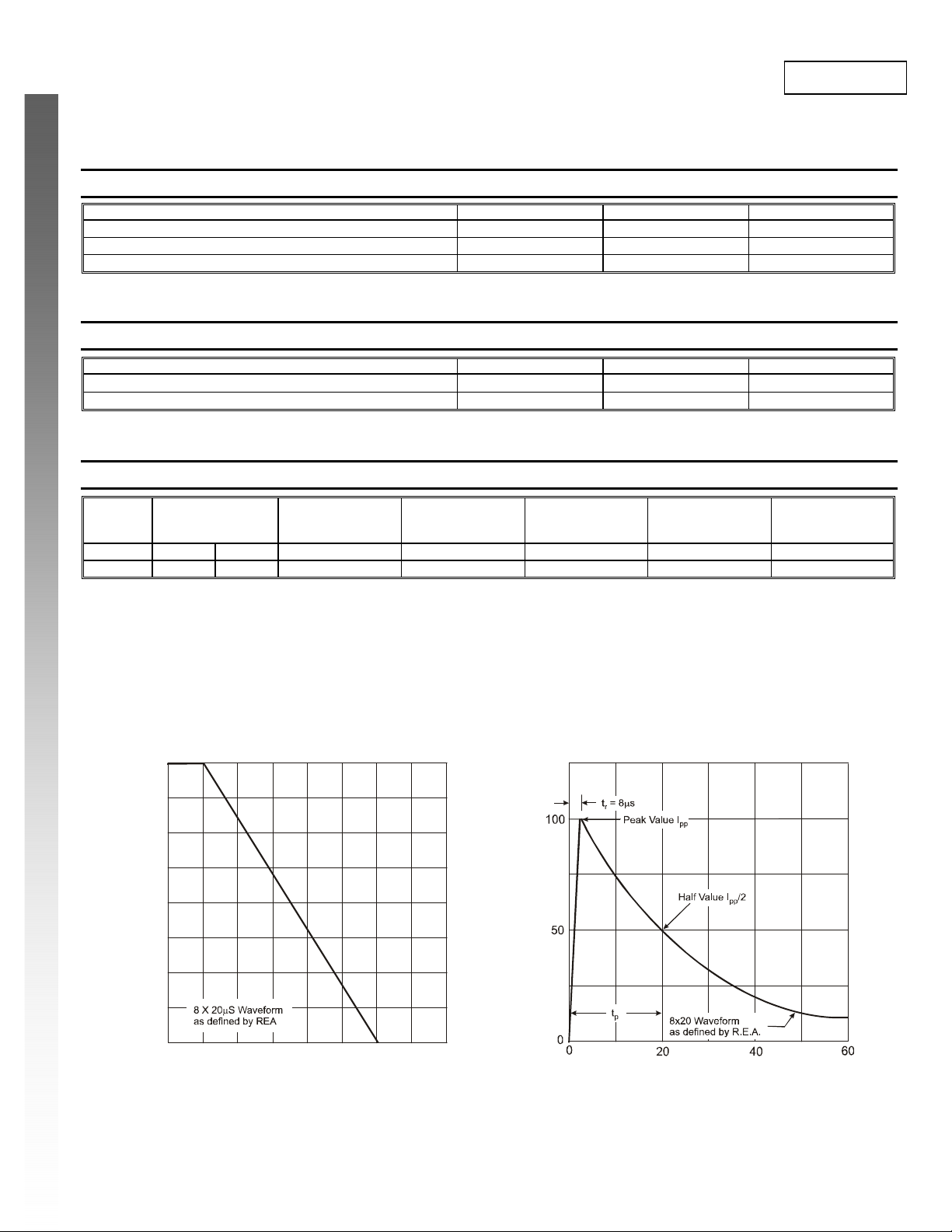
IN %
IN
A
50
LSE DE
25
PEAK POWER OR CURRENT
EAK
PP pp
I , PEAK PULSE CURRENT (%I )
0
0 25 50 75 100 125 150 175 200
T , AMBIENT TEMPERATURE ( C)
A
°
Figure 1. Pulse Derating Curve
t, TIME (µs)
Figure 2. Pulse Waveform
DLPT05W
Document number: DS35592 Rev. 3 - 2
2 of 5
www.diodes.com
June 2012
© Diodes Incorporated
Page 3

NEW PRODUCT
DLPT05W
1.5
1.4
1.3
1.2
1.1
1.0
0.9
10
T = 25C
°
J
Non Repetitive
Pulse Wave f orm
Note 7
1
0.1
0.8
T
0.7
C , TOTAL CAPACITANCE (pF)
0.6
0.5
05.53.50.5 1.0 1.5 2.0 2.5 3.0 4.0 4.5 5.0
V REVERSE VOLTAGE (V)
Figure 3. Typical Total Capacitance vs. Reverse Voltage
R,
D
P , PEAK PULSE POWER (kW)
0.01
0.1 1.0
10
tp, PULSE WIDTH (µs)
Figure 4. Pulse Rating Curve
100
1,000
Typical Application Schematics
Transmission Line
Rg
Driver
Driver
Rg
Vcc
Vcc
I/O Line 1
I/O Line 1
Transmission Line
Figure 5. Data Line Terminator
Vcc
Vcc
Vcc
Vcc
IC
IC
Vcc
Vcc
DLPT05W
Document number: DS35592 Rev. 3 - 2
I/O Line 2
I/O Line 2
Figure 6. Data Line Protection
3 of 5
www.diodes.com
June 2012
© Diodes Incorporated
Page 4
Package Outline Dimensions
K
J
NEW PRODUCT
Suggested Pad Layout
Z
DLPT05W
A
Dim Min Max Typ
C
B
A 0.25 0.40 0.30
B 1.15 1.35 1.30
C 2.00 2.20 2.10
G
H
D - - 0.65
G 1.20 1.40 1.30
H 1.80 2.20 2.15
J 0.0 0.10 0.05
M
K 0.90 1.00 1.00
L 0.25 0.40 0.30
D
Y
L
M 0.10 0.18 0.11
α
Dimensions Value (in mm)
C
X
E
SOT323
0° 8° -
All Dimensions in mm
Z 2.8
X 0.7
Y 0.9
C 1.9
E 1.0
DLPT05W
Document number: DS35592 Rev. 3 - 2
4 of 5
www.diodes.com
June 2012
© Diodes Incorporated
Page 5

DIODES INCORPORATED MAKES NO WARRANTY OF ANY KIND, EXPRESS OR IMPLIED, WITH REGARDS TO THIS DOCUMENT,
INCLUDING, BUT NOT LIMITED TO, THE IMPLIED WARRANTIES OF MERCHANTABILITY AND FITNESS FOR A PARTICULAR PURPOSE
(AND THEIR EQUIVALENTS UNDER THE LAWS OF ANY JURISDICTION).
Diodes Incorporated and its subsidiaries reserve the right to make modifications, enhancements, improvements, corrections or other changes
without further notice to this document and any product described herein. Diodes Incorporated does not assume any liability arising out of the
application or use of this document or any product described herein; neither does Diodes Incorporated convey any license under its patent or
trademark rights, nor the rights of others. Any Customer or user of this document or products described herein in such applications shall assume
all risks of such use and will agree to hold Diodes Incorporated and all the companies whose products are represented on Diodes Incorporated
website, harmless against all damages.
Diodes Incorporated does not warrant or accept any liability whatsoever in respect of any products purchased through unauthorized sales channel.
Should Customers purchase or use Diodes Incorporated products for any unintended or unauthorize d application, Customers shall indemnify and
hold Diodes Incorporated and its representatives harmless against all claims, damages, expenses, and attorney fees arising out of, directly or
indirectly, any claim of personal injury or death associated with such unintended or unauthorized application.
Products described herein may be covered by one or more United States, international or foreign patents pending. Product names and markings
noted herein may also be covered by one or more United States, international or foreign trademarks.
NEW PRODUCT
Diodes Incorporated products are specifically not authorized for use as critical components in life support devices or systems without the express
written approval of the Chief Executive Officer of Diodes Incorporated. As used herein:
A. Life support devices or systems are devices or systems which:
1. are intended to implant into the body, or
labeling can be reasonably expected to result in significant injury to the user.
B. A critical component is any component in a life support device or system whose failure to perform can be reasonably expected to cause the
failure of the life support device or to affect its safety or effectiveness.
Customers represent that they have all necessary expertise in the safety and regulatory ramifications of their life support devices or systems, and
acknowledge and agree that they are solely responsible for all legal, regulatory and safety-related requirements concerning their products and any
use of Diodes Incorporated products in such safety-critical, life support devices or systems, notwithstanding any devices- or systems-related
information or support that may be provided by Diodes Incorporated. Further, Customers must fully indemnify Diodes Incorporated and its
representatives against any damages arising out of the use of Diodes Incorporated products in such safety-critical, life support devices or systems.
Copyright © 2012, Diodes Incorporated
www.diodes.com
2. support or sustain life and whose failure to perform when properly used in accordance with instructions for use provided in the
IMPORTANT NOTICE
LIFE SUPPORT
DLPT05W
DLPT05W
Document number: DS35592 Rev. 3 - 2
5 of 5
www.diodes.com
June 2012
© Diodes Incorporated
 Loading...