

Page 1
/
/
/
A
Please click here to visit our online spice models database.
DATA BUS TRANSIENT SUPPRESSOR / 3-PHASE FULL WAVE BRIDGE RECTIFIER
Features
• Fast Switching Speed
• Ultra-Small Surface Mount Package
• Ideal For Three Dataline Rail Clamp or Three Phase Full Wave
Bridge Rectification
• Lead Free By Design/RoHS Compliant (Note 4)
• "Green" Device (Note 5)
Data Line Transient Protection
In accordance with (Note 1):
• IEC 61000-4-2 Contact Method: ±15kV
• IEC 61000-4-2 Air Discharge Method: ±25kV
Maximum Ratings @T
= 25°C unless otherwise specified
A
Characteristic Symbol Value Unit
Peak Repetitive Reverse Voltage
Working Peak Reverse Voltage
DC Blocking Voltage
RMS Reverse Voltage
Forward Current (Single Diode)
Non-Repetitive Peak Forward Surge Current @ t = 1.0μs
@ t = 1.0ms
@ t = 1.0s
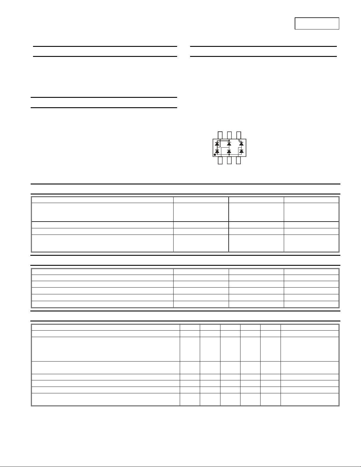
TOP VIEW
Mechanical Data
• Case: SOT-363
• Case Material: Molded Plastic, "Green" Molding Compound.
UL Flammability Classification Rating 94V-0 (Note 4)
• Moisture Sensitivity: Level 1 per J-STD-020D
• Terminals: Finish ⎯ Matte Tin annealed over Alloy 42
Leadframe. Solderable per MIL-STD-202, Method 208
• Ordering Information: See Page 2
• Marking Information: See Page 2
• Weight: 0.006 grams (approximate)
SOT-363
V
RRM
V
RWM
VR
V
R(RMS)
IFM
I
FSM
DC
3
+
V
3
CC
GND
1
/
/
DC-
1
TOP VIEW
DC
+
V
CC
DL
2
/
C
2
AC
DL
DL
AC
Internal Schematic
DLPA006
85 V
60 V
160 mA
4.0
1.0
0.5
A
Thermal Characteristics
Characteristic Symbol Value Unit
Power Dissipation (Note 2)
Power Dissipation (Note 3)
Thermal Resistance Junction to Ambient Air (Note 2)
Thermal Resistance Junction to Ambient Air (Note 3)
Operating and Storage Temperature Range
Electrical Characteristics @T
Characteristic Symbol Min Typ Max Unit Test Condition
Reverse Breakdown Voltage (Note 6)
Forward Voltage
Leakage Current (Note 6)
Total Capacitance (per element)
Capacitance Between Two Data Lines (DL1 & DL2, DL1 & DL3) CLL ⎯
Capacitance Between Data Line and Ground
Reverse Recovery Time
Notes: 1. Tested with VCC pins connected to GND pin.
6. Short duration pulse test used to minimize self-heating.
DLPA006
Document number: DS30665 Rev. 8 - 2
2. Device mounted on FR-4 PCB, 1 inch x 0.85 inch x 0.062 inch; pad layout as shown on Diodes Inc. suggested pad layout document AP02001, which
can be found on our website at http://www.diodes.com/datasheets/ap02001.pdf.
3. Device mounted on Alumina PCB, 0.4 inch x 0.3 inch x 0.024 inch; pad layout as shown on Diodes Inc. suggested pad layout document AP02001, which
can be found on our website at http://www.diodes.com/datasheets/ap02001.pdf.
4. No purposefully added lead.
5. Diodes Inc.'s "Green" policy can be found on our website at http://www.diodes.com/products/lead_free/index.php.
A
PD
PD
R
θ
R
θ
TJ, T
= 25°C unless otherwise specified
V
(BR)R
VF
IR ⎯ ⎯
CT ⎯
C
⎯
LG
trr ⎯ ⎯
1 of 4
www.diodes.com
JA
JA
STG
85
⎯ ⎯
200 mW
300 mW
625
417
-65 to +150
⎯ ⎯
0.90
1.0
1.1
1.25
5.0
80
2
⎯
1.6 2.6 pF
2.5 3.5 pF
3.0
V
IR = 100μA
IF = 1.0mA
IF = 10mA
V
IF = 50mA
IF = 150mA
VR = 75V
nA
nA
VR = 75V, TJ = 150°C
pF
VR = 0, f = 1.0MHz
VR = 0, f = 1.0MHz
VR = 0, f = 1.0MHz
IF = IR = 10mA,
μs
I
°C/W
°C/W
°C
= 0.1 x IR, RL = 100Ω
rr
October 2008
© Diodes Incorporated
Page 2
P, P
OWER
PATIO
N
TANT
O
US F
O
R
RD CUR
RENT
TANT
O
US R
R
CUR
RENT
DLPA006
(mA)
WA
ANE
F
I , INS
1,000
100
10
1.0
0.1
0.01
01
V , INSTANTANEOUS FORWARD VOLTAGE (V)
F
Fig. 2 Typical Forward Characteristics, Per Element
2
300
250
(mW)
200
150
DISSI
100
D
50
0
0 25 50 75 100 125 150
T , AMBIENT TEMPERA TURE (°C)
A
Fig. 1 Power Derating Curve, T otal Package
10
(nA )
SE
EVE
1
ANE
R
I , INS
0.1
050
T , AMBIENT TEMPERA TURE ( C)
Fig. 3 Typical Reverse Characteristics, Per Element
A
150100 200
°
Ordering Information (Note 7)
Part Number Case Packaging
DLPA006-7 SOT-363 3000/Tape & Reel
Notes: 7. For packaging details, go to our website at http://www.diodes.com/datasheets/ap02007.pdf.
Marking Information
JAD
Date Code Key
Year 2005 2006 2007 2008 2009 2010 2011 2012
Code S T U V W X Y Z
Month Jan Feb Mar Apr May Jun Jul Aug Sep Oct Nov Dec
Code 1 2 3
4 5 6 7 8 9 O N D
DLPA006
Document number: DS30665 Rev. 8 - 2
www.diodes.com
JAD = Product Type Marking Code
YM = Date Code Marking
Y = Year (ex: S = 2005)
YM
M = Month (ex: 9 = September)
2 of 4
October 2008
© Diodes Incorporated
Page 3

Typical Applications
Data Line Bus Transient Suppressor
Three Phase, Full-Wave Bridge Rectifier
Package Outline Dimensions
A
K
H
J
Suggested Pad Layout
G
Z
Y
X
DLPA006
V/V
BUS CC
DL
1
3-Phase
AC source
B C
D
L
F
EE
DL
Ground
C
2
DC-
M
DL
AC
1
AC
2
AC
3
Dimensions
3
DC+
+
Load
-
SOT-363
Dim
Min Max
A 0.10 0.30
B 1.15 1.35
C 2.00 2.20
D 0.65 Nominal
0.30 0.40
F
H 1.80 2.20
J
⎯
0.10
K 0.90 1.00
L 0.25 0.40
M 0.10 0.25
α
0° 8°
All Dimensions in mm
Value (in mm)
Z
G
2.5
1.3
X 0.42
Y
C
E
0.6
1.9
0.65
DLPA006
Document number: DS30665 Rev. 8 - 2
3 of 4
www.diodes.com
October 2008
© Diodes Incorporated
Page 4

IMPORTANT NOTICE
Diodes Incorporated and its subsidiaries reserve the right to make modifications, enhancements, improvements, corrections or other changes
without further notice to any product herein. Diodes Incorporated does not assume any liability arising out of the application or use of any product
described herein; neither does it convey any license under its patent rights, nor the rights of others. The user of products in such applications shall
assume all risks of such use and will agree to hold Diodes Incorporated and all the companies whose products are represented on our website,
harmless against all damages.
LIFE SUPPORT
Diodes Incorporated products are not authorized for use as critical components in life support devices or systems without the expressed written
approval of the President of Diodes Incorporated.
DLPA006
DLPA006
Document number: DS30665 Rev. 8 - 2
4 of 4
www.diodes.com
October 2008
© Diodes Incorporated
 Loading...