Diodes DFLU1400 User Manual

®
Features
Glass Passivated Die Construction
Super-Fast Recovery Time for High Efficiency
Low Forward Voltage Drop and High Current Capability
Patented Interlocking Clip Design for High Surge Current
Capacity
Lead-Free Finish; RoHS Compliant (Notes 1 & 2)
Halogen and Antimony Free. “Green” Device (Note 3)
Qualified to AEC-Q101 Standards for High Reliability
Green
1.0A SURFACE MOUNT SUPER-FAST RECTIFIER
Mechanical Data
Case: PowerDI®123
Case Material: Molded Plastic, "Green" Molding
Compound. UL Flammability Classification Rating 94V-0
Moisture Sensitivity: Level 1 per J-STD-020C
Terminal Connections: Cathode Band
Terminals: Finish – Matte Tin annealed over Copper
leadframe. Solderable per MIL-STD-202, Method 208
Weight: 0.011 grams (approximate)
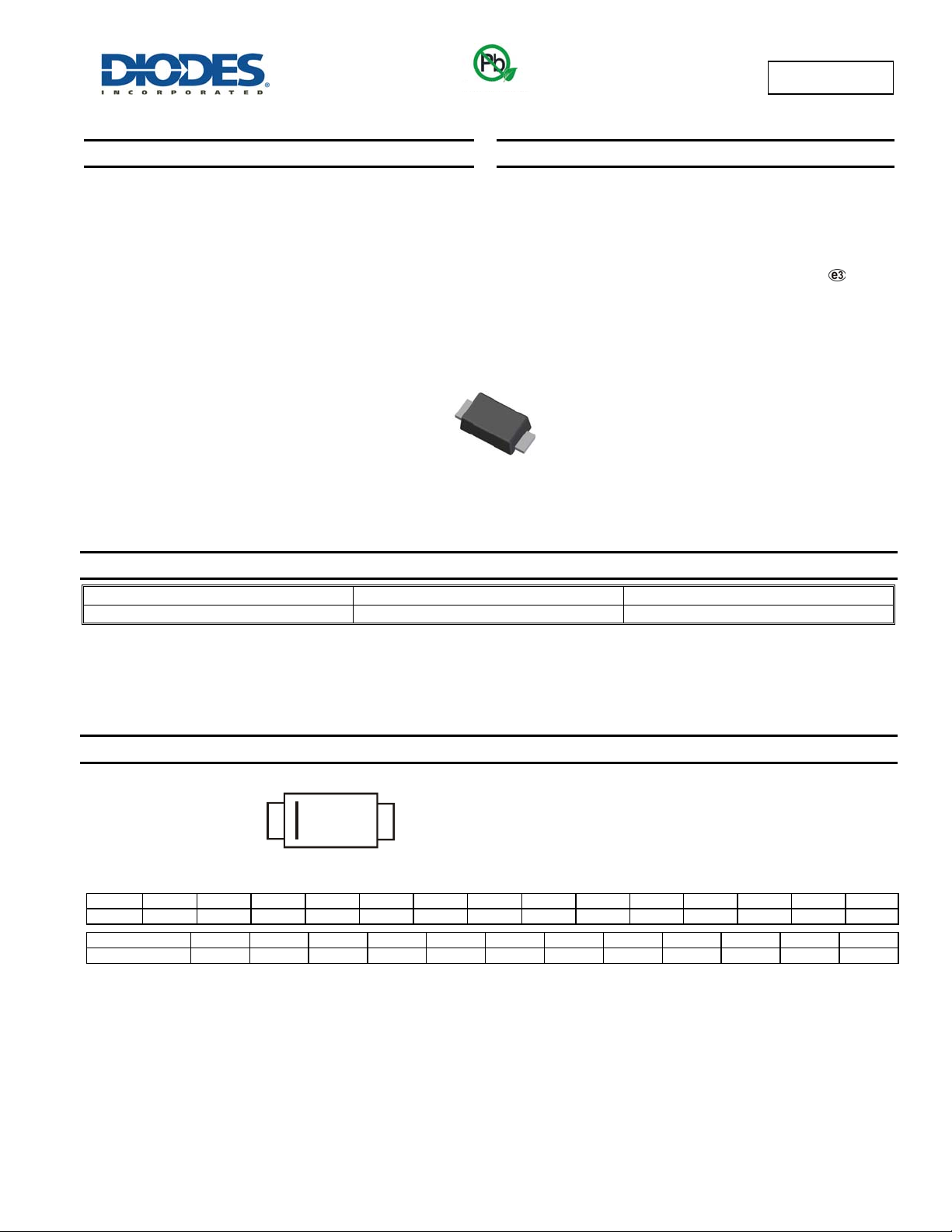
Top View
DFLU1400
PowerDI®123
Ordering Information (Note 4)
Device
DFLU1400-7
Notes: 1. EU Directive 2002/95/EC (RoHS) & 2011/65/EU (RoHS 2) compliant. All applicable RoHS exemptions applied.
2. See http://www.diodes.com/quality/lead_free.html for more information about Diodes Incorporated’s definitions of Halogen- and Antimony-free, "Green"
and Lead-free.
3. Halogen- and Antimony-free "Green” products are defined as those which contain <900ppm bromine, <900ppm chlorine (<1500ppm total Br + Cl) and
<1000ppm antimony compounds.
4. For packaging details, go to our website at http://www.diodes.com/products/packages.html
Packaging Shipping
PowerDI
123 3000/Tape & Reel
Marking Information
Date Code Key
Year 2005 2006 2007 2008 2009 2010 2011 2012 2013 2014 2015 2016 2017 2018
Code S T U V W X Y Z A B C D E F
Month Jan Feb Mar Apr May Jun Jul Aug Sep Oct Nov Dec
Code 1 2 3 4 5 6 7 8 9 O N D
F16
YM
DFLU1400
Document number: DS30784 Rev. 3 - 2
F16 = Product Type Marking Code
YM = Date Code Marking
Y = Year (ex: A = 2013)
M = Month (ex: 9 = September)
1 of 5
www.diodes.com
June 2013
© Diodes Incorporated

)
r
Maximum Ratings (@T
= +25°C, unless otherwise specified.)
A
Single phase, half wave, 60Hz, resistive or inductive load.
For capacitive load, derate current by 20%.
Characteristic Symbol Value Unit
V
Peak Repetitive Reverse Voltage
Working Peak Reverse Voltage
DC Blocking Voltage (Note 9)
RMS Reverse Voltage
Average Rectified Output Current
Non-Repetitive Peak Forward Surge Current 8.3ms
Single Half Sine-Wave Superimposed on Rated Load
V
V
R(RMS
I
RRM
RWM
VR
IO
FSM
Thermal Characteristics
Characteristic Symbol Typ Max Unit
Power Dissipation (Note 5) @TA = +25°C PD
Thermal Resistance Junction to Ambient (Note 5) @TA = +25°C
Thermal Resistance Junction to Soldering Point (Note 7)
Operating and Storage Temperature Range
R
R
T
j, TSTG
Θ
JA
Θ
JS
117
DFLU1400
400 V
280 V
1.0 A
30 A
1.0 W
6 °C/W
-65 to +150
°C/W
C
Electrical Characteristics (@T
= +25°C, unless otherwise specified.)
A
Characteristic Symbol Value Unit
Maximum Forward Voltage Drop @IF = 1.0A VFM
Peak Reverse Current @TA = +25C
at Rated DC Blocking Voltage (Note 9) @TA = +100C
Maximum Reverse Recovery Time (Note 8)
IRM
t
r
Typical Total Capacitance (f = 1MHz, VR = 4VDC) CT
Notes: 5. Device mounted on 1" x 1", Polymide PCB; 2 oz. Cu pad layout as shown on Diodes Inc. suggested pad layout document AP02001.pdf.
6. RoHS revision 13.2.2003. Glass and high temperature solder exemptions applied, see EU Directive Annex Notes 5 and 7.
7. Theoretical R
8. Measured with I
9. Short duration pulse test used to minimize self-heating effect.
10. Device mounted on FR-4 PCB, 2oz. Cu pad layout as shown on Diodes Inc. suggested pad layout document AP02001.pdf. (see page 2)
DFLU1400
Document number: DS30784 Rev. 3 - 2
calculated from the top center of the die straight down to the PCB cathode tab solder junction.
JS
= 0.5A, IR = 1.0A, Irr = 0.25A. See figure 5.
F
2 of 5
www.diodes.com
1.25 V
5.0
200
A
25 ns
14 pF
© Diodes Incorporated
June 2013
 Loading...