

Page 1
A
225W SURFACE MOUNT TRANSIENT VOLTAGE SUPPRESSOR
Features
225W Peak Pulse Power Dissipation (10µs x 1000µs waveform)
5.0V - 220V Standoff Voltages
Excellent Clamping Capability
Lead-Free Finish; RoHS Compliant (Notes 1 & 2)
Halogen and Antimony Free. “Green” Device (Note 3)
Qualified to AEC-Q101 Standards for High Reliability
Patented Interlocking Clip Design for High Surge Capacity,
US Patent #7,095,113
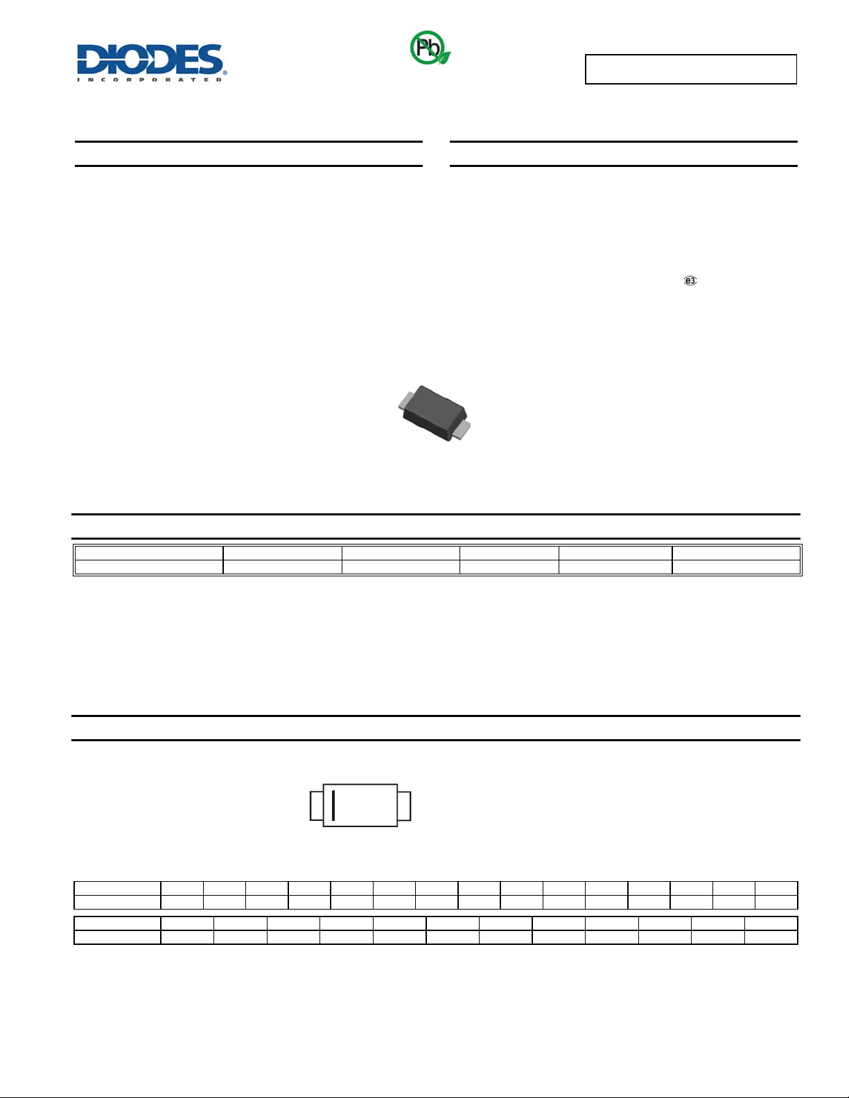
POWERDI123
Green
DFLT5V0A –DFLT220
Mechanical Data
Case: POWERDI123
Case Material: Molded Plastic, "Green" Molding Compound.
UL Flammability Classification Rating 94V-0
Moisture Sensitivity: Level 1 per J-STD-020
Terminal Connections: Cathode Band
Terminals: Finish Matte Tin annealed over Copper leadframe.
Solderable per MIL-STD-202, Method 208
Weight: 0.01 grams (approximate)
Top View
POWERDI
Ordering Information (Note 4)
Product Compliance Marking Reel size(inches) Tape width(mm) Quantity per reel
DFLTxxxA-7* AEC-Q101 Fxx 7 8 3,000/Tape & Reel
* Add "-7" to the appropriate type number in Electrical Characteristics Table on page 2. Example: 10V reverse standoff device = DFLT10A-7.
Notes: 1. No purposely added lead. Fully EU Directive 2002/95/EC (RoHS) & 2011/65/EU (RoHS 2) compliant.
2. See http://www.diodes.com/quality/lead_free.html for more information about Diodes Incorporated’s definitions of Halogen- and Antimony-free, "Green"
and Lead-free.
3. Halogen- and Antimony-free "Green” products are defined as those which contain <900ppm bromine, <900ppm chlorine (<1500ppm total Br + Cl) and
<1000ppm antimony compounds.
4. For packaging details, go to our website at http://www.diodes.com/products/packages.html
Marking Information
Date Code Key
Year 2004 2005 2006 2007 2008 2009 2010 2011 2012 2013 2014 2015 2016 2017 2018
Code R S T U V W X Y Z A B C D E F
Month Jan Feb Mar Apr May Jun Jul Aug Sep Oct Nov Dec
Code 1 2 3 4 5 6 7 8 9 O N D
Fxx
YM
Fxx = Product Type Marking Code,
See Electrical Characteristics Table on Page 2
YM = Date Code Marking
Y = Year (ex: R = 2004)
M = Month (ex: 9 = September)
POWERDI is a registered trademark of Diodes Incorporated.
DFLT5V0A – DFLT220A
Document number: DS30581 Rev. 8 - 2
1 of 5
www.diodes.com
June 2013
© Diodes Incorporated
Page 2
A
pp
DFLT5V0A –DFLT220
Maximum Ratings (@T
= +25°C, unless otherwise specified.)
A
Characteristic Symbol Value Unit
Peak Pulse Power Dissipation (Note 5) 10/1000µs
(Note 6) 8/20µs
Peak Forward Surge Current, 8.3ms Single Half Sine Wave (Note 7)
P
I
FSM
PK
Instantaneous Forward Voltage @ IPP = 12A (Note 8) VF
225
1125
W
50 A
3.5 V
Thermal Characteristics
Characteristic Symbol Value Unit
DC Steady-State Power Dissipation (Note 9)
Thermal Resistance, Junction to Ambient (Note 9)
Thermal Resistance, Junction to Soldering Point (Note 10)
Operating and Storage Temperature Range
P
D
R
θJA
R
θJS
T
, T
J
STG
Electrical Characteristics (@T
Reverse
Part Number
Standoff
Voltage
V
(V)
RWM
V
Min (V) Max (V)
= +25°C, unless otherwise specified.)
A
Breakdown
Voltage
@ IT (Note 11)
BR
Test
Current
IT (mA) IR (A) VC (V)
Max. Reverse
Leakage @ V
RWM
Max. Clamping
Voltage @ Ipp
DFLT5V0A 5.0 6.40 7.0 10 400 9.2 24.5 FAE
DFLT6V0A 6.0 6.67 7.37 10 400 10.3 21.8 FAG
DFLT6V5A 6.5 7.22 7.98 10 250 11.2 20.1 FAK
DFLT7V0A 7.0 7.78 8.60 10 100 12.0 18.8 FAM
DFLT7V5A 7.5 8.33 9.21 1.0 50 12.9 17.4 FAP
DFLT8V0A 8.0 8.89 9.83 1.0 25 13.6 16.5 FAR
DFLT8V5A 8.5 9.44 10.4 1.0 10 14.4 15.6 FAT
DFLT9V0A 9.0 10.0 11.1 1.0 5.0 15.4 14.6 FAV
DFLT10A 10 11.1 12.3 1.0 2.5 17.0 13.2 FAX
DFLT11A 11 12.2 13.5 1.0 2.5 18.2 12.4 FAZ
DFLT12A 12 13.3 14.7 1.0 2.5 19.9 11.3 FBE
DFLT13A 13 14.4 15.9 1.0 1.0 21.5 10.5 FBG
DFLT14A 14 15.6 17.2 1.0 1.0 23.2 9.7 FBK
DFLT15A 15 16.7 18.5 1.0 1.0 24.4 9.22 FBM
DFLT16A 16 17.8 19.7 1.0 1.0 26.0 8.65 FBP
DFLT17A 17 18.9 20.9 1.0 1.0 27.6 8.15 FBR
DFLT18A 18 20.0 22.1 1.0 1.0 29.2 7.71 FBT
DFLT20A 20 22.2 24.5 1.0 1.0 32.4 6.94 FBV
DFLT22A 22 24.4 26.9 1.0 1.0 35.5 6.34 FBX
DFLT24A 24 26.7 29.5 1.0 1.0 38.9 5.78 FBZ
DFLT26A 26 28.9 31.9 1.0 1.0 42.1 5.35 FCE
DFLT27A 27 30 33.15 1.0 1.0 43.7 5.15 FCF
DFLT28A 28 31.1 34.4 1.0 1.0 45.4 4.96 FCG
DFLT30A 30 33.3 36.8 1.0 1.0 48.4 4.65 FCK
DFLT33A 33 36.7 40.6 1.0 1.0 53.3 4.22 FCM
DFLT36A 36 40.0 44.2 1.0 1.0 58.1 3.87 FCP
DFLT40A 40 44.4 49.1 1.0 1.0 64.5 3.49 FCR
DFLT43A 43 47.8 52.8 1.0 1.0 69.4 3.24 FCT
DFLT45A 45 50.0 55.3 1.0 1.0 72.7 3.10 FCV
DFLT48A 48 53.3 58.9 1.0 1.0 77.4 2.91 FCX
DFLT51A 51 56.7 62.7 1.0 1.0 82.4 2.73 FCZ
DFLT170A 170 189 209 1.0 5.0 281 0.81 FDZ
DFLT220A 220 242 276 1.0 5.0 375 0.60 FEZ
Notes: 5. Non-Repetitive current pulse as shown in figure 2 and derated above TA = +25°C as per figure 1.
6. Non-Repetitive current pulse as shown in figure 3 and derated above T
7. I
8. 1/2 sine wave (or equivalent square wave), pulse width = 8.3ms, duty cycle = 4 pulses/minute maximum.
9. Device mounted on 1"x1", FR-4 PCB; 2 oz. Cu pad layout. Cathode pad dimensions 5.5mm x 3.5mm. Anode pad dimensions 2.25mm x 3.5mm.
10. Theoretical R
11. V
POWERDI is a registered trademark of Diodes Incorporated.
DFLT5V0A – DFLT220A
Document number: DS30581 Rev. 8 - 2
= 40A for DFLT170A and DFLT220A; I
FSM
calculated from the top center of the die straight down to the PCB/cathode tab solder junction.
measured at pulse test current IT with tp 5.0ms at TA = +25°C.
BR
JS
= 50A for all other voltages.
FSM
www.diodes.com
= +25°C as per figure 1.
A
2 of 5
1.0 W
125 °C/W
6 °C/W
-65 to +150
C
Max. Peak
Pulse Current
I
Marking
Code
(A)
June 2013
© Diodes Incorporated
Page 3

A
P
P
U
RAT
G
O
P ST
Y
T
T
P
OWER
PAT
O
DFLT5V0A –DFLT220
100
F
Peak Value I
pp
75
IN %
IN
50
Half Value I /2
pp
LSE DE
25
PEAK POWER OR CURRENT
EAK
0
0 25 50 75 100 125 150 175 200
T , AMBIENT TEMPERATURE ( C)
A
Fig. 1 Pulse Derating Curve
Peak Value I
pp
°
I , PEAK PULSE CURRENT (%I )
PP pp
100
t
p
0
10 X 1000 Waveform
as defined by R.E.A.
1
2
3
t, TIME (ms)
Fig. 2 Pulse Waveform
T = 25C
J
Non Repetitive
Pulse Wave f orm
Shown in Fig. 3
°
10
Half Value I /2
pp
1.0
D
PP pp
I , PEAK PULSE CURRENT (%I )
t
p
8x20 Waveform
as defined by R.E.A.
1.2
N (W)
I
1.0
0.8
DISSI
0.6
E
A
0.4
S
EAD
0.2
P , PEAK PULSE POWER (kW)
1,600
1,400
)
1,200
F
p
(
E
1,000
C
N
A
T
I
C
A
P
A
C
L
A
T
O
T
0.1
800
600
400
0.1
1.0
10
t , PULSE WIDTH (µs)
p
Fig. 4 Puls e Rating Curve
100
1,000
10,000
200
(AV),
0
025
T , TERMINAL TEMPERATURE ( C)
50
T
75
Fig. 5 Steady State Power Derating Curve
100
125 150
°
0
0
10
20 30
40
50
60
TOTAL CAPACITANCE
Fig. 6 V (V)
RWM
POWERDI is a registered trademark of Diodes Incorporated.
DFLT5V0A – DFLT220A
Document number: DS30581 Rev. 8 - 2
3 of 5
www.diodes.com
June 2013
© Diodes Incorporated
Page 4

A
C, T
O
T
CAPACITANC
70
70
65
60
f = 1MHz
60
55
50
E (pF)
50
45
40
40
35
30
T
C , TOT AL CAPACITANCE (pF)
20
DFLT170A
AL
30
25
T
20
15
10
0123 456
V , DC REVERSE VOLTAGE (V)
R
Fig. 7 Total Cap acitance vs. Reverse Voltage
10
0 5 10 15 20 25 30 35 40
Fig. 8 Total Capacitance vs. Reverse Voltage
Package Outline Dimensions
Please see AP02002 at http://www.diodes.com/datasheets/ap02002.pdf for latest version.
B
C
E
Dim Min Max Typ
A 3.50 3.90 3.70
B 2.60 3.00 2.80
C 1.63 1.93 1.78
D
L
L1
H
L3
D 0.93 1.00 0.98
E 0.85 1.25 1.00
H 0.15 0.25 0.20
L 0.40 0.50 0.45
L1 - - 1.35
L2 - - 1.10
E
L2
A
E
L3 - - 0.20
All Dimensions in mm
Suggested Pad Layout
Please see AP02001 at http://www.diodes.com/datasheets/ap02001.pdf for the latest version.
X1 G
X2
Y2
Y1
Dimensions Value (in mm)
DFLT5V0A –DFLT220
DFLT220A
V , DC REVERSE VOLTAGE (V)
R
POWERDI123
G 1.0
X1 2.2
X2 0.9
Y1 1.4
Y2 1.4
f = 1MHz
POWERDI is a registered trademark of Diodes Incorporated.
DFLT5V0A – DFLT220A
Document number: DS30581 Rev. 8 - 2
4 of 5
www.diodes.com
June 2013
© Diodes Incorporated
Page 5

A
IMPORTANT NOTICE
DIODES INCORPORATED MAKES NO WARRANTY OF ANY KIND, EXPRESS OR IMPLIED, WITH REGARDS TO THIS DOCUMENT,
INCLUDING, BUT NOT LIMITED TO, THE IMPLIED WARRANTIES OF MERCHANTABILITY AND FITNESS FOR A PARTICULAR PURPOSE
(AND THEIR EQUIVALENTS UNDER THE LAWS OF ANY JURISDICTION).
Diodes Incorporated and its subsidiaries reserve the right to make modifications, enhancements, improvements, corrections or other changes
without further notice to this document and any product described herein. Diodes Incorporated does not assume any liability arising out of the
application or use of this document or any product described herein; neither does Diodes Incorporated convey any license under its patent or
trademark rights, nor the rights of others. Any Customer or user of this document or products described herein in such applications shall assume
all risks of such use and will agree to hold Diodes Incorporated and all the companies whose products are represented on Diodes Incorporated
website, harmless against all damages.
Diodes Incorporated does not warrant or accept any liability whatsoever in respect of any products purchased through unauthorized sales channel.
Should Customers purchase or use Diodes Incorporated products for any unintended or unauthorize d application, Customers shall indemnify and
hold Diodes Incorporated and its representatives harmless against all claims, damages, expenses, and attorney fees arising out of, directly or
indirectly, any claim of personal injury or death associated with such unintended or unauthorized application.
Products described herein may be covered by one or more United States, international or foreign patents pending. Product names and markings
noted herein may also be covered by one or more United States, international or foreign trademarks.
This document is written in English but may be translated into multiple languages for reference. Onl y the English version of this document is the
final and determinative format released by Diodes Incorporated.
LIFE SUPPORT
Diodes Incorporated products are specifically not authorized for use as critical components in life support devices or systems without the express
written approval of the Chief Executive Officer of Diodes Incorporated. As used herein:
A. Life support devices or systems are devices or systems which:
1. are intended to implant into the body, or
2. support or sustain life and whose failure to perform when properly used in accordance with instructions for use provided in the
labeling can be reasonably expected to result in significant injury to the user.
B. A critical component is any component in a life support device or system whose failure to perform can be reasonably expected to cause the
failure of the life support device or to affect its safety or effectiveness.
Customers represent that they have all necessary expertise in the safety and regulatory ramifications of their life support devices or systems, and
acknowledge and agree that they are solely responsible for all legal, regulatory and safety-related requirements concerning their products and any
use of Diodes Incorporated products in such safety-critical, life support devices or systems, notwithstanding any devices- or systems-related
information or support that may be provided by Diodes Incorporated. Further, Customers must fully indemnify Diodes Incorporated and its
representatives against any damages arising out of the use of Diodes Incorporated products in such safety-critical, life support devices or systems.
Copyright © 2013, Diodes Incorporated
www.diodes.com
DFLT5V0A –DFLT220
POWERDI is a registered trademark of Diodes Incorporated.
DFLT5V0A – DFLT220A
Document number: DS30581 Rev. 8 - 2
5 of 5
www.diodes.com
June 2013
© Diodes Incorporated
 Loading...