Features
• Guard Ring Die Construction for Transient Protection
• Low Power Loss, High Efficiency
• Patented Interlocking Clip Design for High Surge Current
Capacity
• Lead Free Finish, RoHS Compliant (Note 1)
• "Green" Molding Compound (No Br, Sb)
• Qualified to AEC-Q101 Standards for High Reliability
DFLS1150
1.0A HIGH VOLTAGE SCHOTTKY BARRIER RECTIFIER
POWERDI
Mechanical Data
• Case: POWERDI®123
• Case Material: Molded Plastic, "Green" Molding Compound. UL
Flammability Classification Rating 94V-0
• Moisture Sensitivity: Level 1 per J-STD-020
• Terminal Connections: Cathode Band
• Terminals: Finish – Matte Tin annealed over Copper Leadframe.
Solderable per MIL-STD-202, Method 208
• Weight: 0.01 grams (approximate)
Top View
®
123
Ordering Information (Note 2)
Part Number Case Packaging
DFLS1150-7
Notes: 1. EU Directive 2002/95/EC (RoHS). All applicable RoHS exemptions applied, see EU Directive 2002/95/EC Annex Notes.
2. For packaging details, go to our website at http://www.diodes.com.
POWERDI
®
123
3000/Tape & Reel
Marking Information
Date Code Key
Year 2004 2005 2006 2007 2008 2009 2010 2011 2012 2013 2014 2015
Code R S T U V W X Y Z A B C
Month Jan Feb Mar Apr May Jun Jul Aug Sep Oct Nov Dec
Code 1 2 3 4 5 6 7 8 9 O N D
POWERDI is a registered trademark of Diodes Incorporated.
F07
YM
DFLS1150
Document number: DS30593 Rev. 7 - 2
F07 = Product Type Marking Code
YM = Date Code Marking
Y = Year (ex: R = 2004)
M = Month (ex: 9 = September)
1 of 4
www.diodes.com
April 2011
© Diodes Incorporated

)
)
θ
θ
(BR)
TANT
O
U
F
O
RWARD CUR
RENT
Maximum Ratings @T
= 25°C unless otherwise specified
A
Single phase, half wave, 60Hz, resistive or inductive load.
For capacitance load, derate current by 20%.
Characteristic Symbol Value Unit
Peak Repetitive Reverse Voltage
Working Peak Reverse Voltage
DC Blocking Voltage
RMS Reverse Voltage
Average Forward Current
Non-Repetitive Peak Forward Surge Current 8.3ms
Single Half Sine-Wave Superimposed on Rated Load
Thermal Characteristics
Characteristic Symbol Typ Max Unit
Thermal Resistance Junction to Soldering Point (Note 3)
Thermal Resistance Junction to Ambient (Note 4) TA = 25°C R
Operating and Storage Temperature Range
T
DFLS1150
V
RRM
V
RWM
V
R
V
R(RMS
I
F(AV
I
FSM
R
JS
JA
, T
J
STG
⎯
125
150 V
106 V
1.0 A
50 A
7
⎯
-55 to +175
°C/W
°C/W
°C
Electrical Characteristics @T
Characteristic Symbol Min Typ Max Unit Test Condition
Reverse Breakdown Voltage (Note 5)
Forward Voltage
Leakage Current (Note 5)
Total Capacitance
Notes: 3. Theoretical R
4. Part mounted on FR-4 board with 2 oz., minimum recommended copper pad layout, which can be found on our website at http://www.diodes.com.
5. Short duration pulse test used to minimize self-heating effect.
10
(A)
1
0.1
0.01
S
0.001
ANE
calculated from the top center of the die straight down to the PCB/cathode tab solder junction.
θJS
= 25°C unless otherwise specified
A
V
R
V
⎯ ⎯
F
I
⎯ ⎯
R
C
⎯
T
150
⎯ ⎯
0.82 V
2
28
⎯
V
μA
pF
IR = 2μA
IF = 1.0A
= 150V, TA = 25°C
V
R
VR = 5VDC, f = 1MHz
0.0001
F
I , INS
0.00001
00.40.5
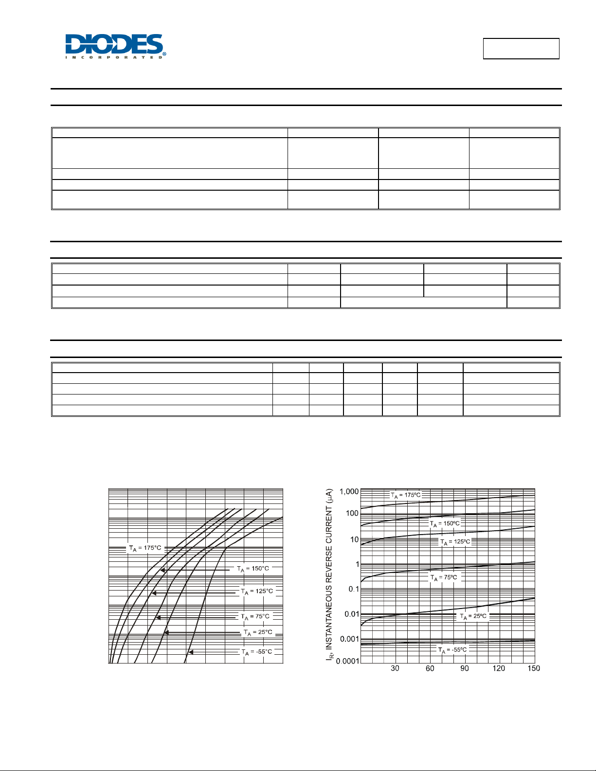
V , INSTANTA NEOUS FORW ARD VOLTAGE (V)
0.20.1
0.3
F
Fig. 1 Typical Forward Characte r is ti cs
0.6 0.7 0.8 0.9
0
V , INSTANTANEOUS REVERSE VOLT AGE (V)
R
Fig. 2 Typical Reverse Characteristics
POWERDI is a registered trademark of Diodes Incorporated.
DFLS1150
Document number: DS30593 Rev. 7 - 2
2 of 4
www.diodes.com
April 2011
© Diodes Incorporated
 Loading...