

Page 1
DF005M - DF10M
1.0A GLASS PASSIVATED BRIDGE RECTIFIERS
Features
• Glass Passivated Die Construction
• Low Forward Voltage Drop, High Current Capability
• Surge Overload Rating to 50A Peak
• Designed for Printed Circuit Board Applications
• UL Listed Under Recognized Component Index, File
Number E94661
• Lead Free Finish, RoHS Compliant (Date Code 0532+)
(Note 3)
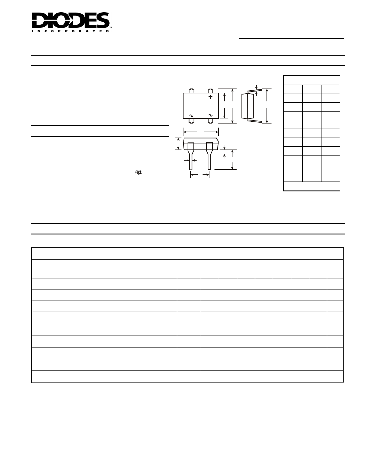
Mechanical Data
• Case: DF-M
• Case Material: Molded Plastic. UL Flammability
Classification Rating 94V-0
• Moisture Sensitivity: Level 1 per J-STD-020C
• Terminals: Finish - Tin. Solder Plated Leads,
Solderable per MIL-STD-202, Method 208
• Polarity: As Marked on Case
• Marking Information: Type Number, See Page 3
• Weight: 0.38 grams (approximate)
H
J
L
K
Maximum Ratings and Electrical Characteristics @T
Single phase, half wave, 60Hz, resistive or inductive load.
For capacitive load, derate current by 20%.
Characteristic Symbol
Peak Repetitive Reverse Voltage
Working Peak Reverse Voltage
DC Blocking Voltage
RMS Reverse Voltage
V
V
V
RMM
RWM
V
RMS
DF
005M
50 100 200 400 600 800 1000 V
R
35 70 140 280 420 580 700 V
C
A
B
E
D
G
= 25°C unless otherwise specified
A
DF
01M
DF
02M
DF
04M
DF
06M
DF-M
Dim Min Max
A 7.40 7.90
B 6.20 6.50
C 0.22 0.30
D 1.27 2.03
E 7.60 8.90
G 3.81 4.69
H 8.13 8.51
J 2.40 3.40
K 5.00 5.20
L 0.46 0.58
All Dimensions in mm
DF
08M
DF
10M
Unit
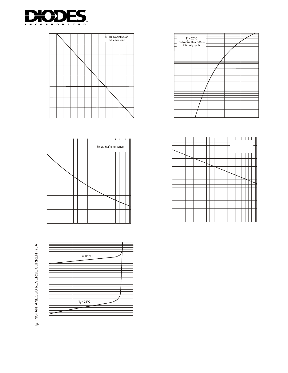
Average Rectified Output Current @ TA = 40°C I
Non-Repetitive Peak Forward Surge Current, 8.3 ms
Single Half Sine-Wave Superimposed on Rated Load
Forward Voltage (per element) @ IF = 1.0 A V
Peak Reverse Current @ TA = 25°C
at Rated DC Blocking Voltage (per element) @ TA = 125°C
I2t Rating for Fusing (t<8.3ms) I2t 10.4 A2s
Typical Total Capacitance per element (Note 1)
Typical Thermal Resistance, Junction to Ambient (Note 2)
Operating and Storage Temperature Range
Notes: 1. Measured at 1.0MHz and applied reverse voltage of 4.0V DC.
DS21201 Rev. 15 - 2
2. Thermal Resistance, junction to ambient, measured on PC board with 5.0mm
3. RοHS revision 13.2.2003. Glass and high temperature solder exemptions applied, see EU Directive Annex Notes 5 and 7.
www.diodes.com
I
FSM
I
C
R
Tj, T
1 of 3
RM
θ
O
FM
T
JA
STG
2
(0.03mm thick) land areas.
1.0 A
50 A
1.1 V
10
500
25 pF
40 °C/W
-65 to +150 °C
DF005M-DF10M
© Diodes Incorporated
µA
Page 2
TANT
O
US FOR
RD C
URRENT
P
O
RWAR
URGE CUR
RENT
C, TOT
CAPACITANC
F
1.0
0.5
(AV)
I , AVERAGE FORWARD CURRENT (A)
0
40
60
T , AMBIENT TEMPERATURE (°C)
A
80
Fig. 1 Output Current Derating Curve
100 120 140
60
(A)
50
10
(A)
1.0
WA
0.1
ANE
F
I, INS
0.01
0.4
0.6
V , INSTANTANEOUS FORWARD VOLTA GE (V)
F
0.8 1.0
Fig. 2 Typical Forward Characteristics (per element)
100
T = 25°C
j
f = 1.0 Mhz
)
V = 50 mV p-p
sig
E (p
1.2
1.4
40
30
D S
20
10
EAK F
FSM
0
I,
110
NUMBER OF CYCLES AT 60 Hz
Fig. 3 Max Non-Repetitive Peak Forward Surge Current
100
10
1.0
AL
100
10
T
1
110
V , REVERSE VOLT AGE (V)
R
Fig. 4 Typical Total Capacitance (per element)
100
0.1
0.01
200406080100 120 140
PERCENT OF RATED PEAK REVERSE VOLTAGE (%)
Fig. 5 Typ Rev erse Char acteristi cs (per element)
DS21201 Rev. 15 - 2
2 of 3
www.diodes.com
DF005M-DF10M
© Diodes Incorporated
Page 3

Ordering Information (Note 4)
Device*
DFxM
* x = Device type, e.g. DF005M or DF10M, etc.
Notes: 4. For packaging details, visit our website at http://www.diodes.com/datasheets/ap02 007.pdf.
Packaging Shipping
DF-M Tube
Marking Information
XXXXX
YWW
Diodes Incorporated and its subsidiaries reserve the right to make modifications, enhancements, improvements, corrections or other changes
without further notice to any product herein. Diodes Incorporated does not assume any liability arising out of the application or use of any product
described herein; neither does it convey any license under its patent rights, nor the rights of others. The user of products in such applications shall
assume all risks of such use and will agree to hold Diodes Incorporated and all the companies whose products are represented on our website,
harmless against all damages.
Diodes Incorporated products are not authorized for use as critical components in life support devices or systems without the expressed written
approval of the President of Diodes Incorporated.
= Manufacturers’ code marking
XXXXX = Product type marking code, ex: DF10M
YWW = Date code marking
Y = Last d igit of year ex: 2 f or 2002
WW = Week code 01 to 52
IMPORTANT NOTICE
LIFE SUPPORT
DS21201 Rev. 15 - 2
3 of 3
www.diodes.com
DF005M-DF10M
© Diodes Incorporated
 Loading...