

Page 1
A
Features
• Provides ESD Protection per IEC 61000-4-2 Standard:
Air ±30kV, Contact ±30kV
• 1 Channel of ESD Protection
• High Peak Pulse Current per IEC 61000-4-5 Standard
• Low Channel Input Capacitance
• Typically Used in Cellular Handsets, Portable Electronics,
Communication Systems, Computers and Peripherals
• Lead Free/RoHS Compliant (Note 1)
• Halogen and Antimony Free "Green" Device (Notes 2 & 3)
ADVANCE INFORMATION
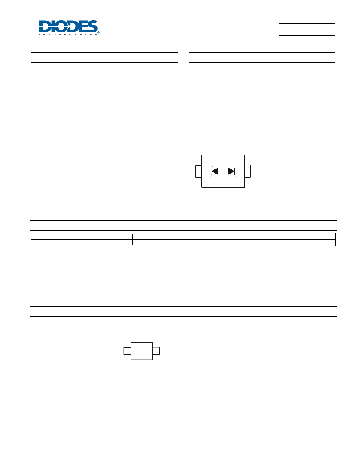
SOD323
Top View
DESD5V0S1BA
LOW CAPACITANCE BIDIRECTIONAL TVS DIODE
Mechanical Data
• Case: SOD323
• Case Material: Molded Plastic, “Green” Molding Compound. UL
Flammability Classification Rating 94V-0
• Moisture Sensitivity: Level 1 per J-STD-020
• Terminals: Matte Tin Finish annealed over Alloy 42 leadframe
(Lead Free Plating). Solderable per MIL-STD-202, Method 208
• Weight: 0.005 grams (approximate)
1
Device Schematic
2
Ordering Information (Note 4)
Part Number Case Packaging
DESD5V0S1BA-7 SOD323 3000/Tape & Reel
Notes: 1. EU Directive 2002/95/EC (RoHS) & 2011/65/EU (RoHS 2) compliant. No purposely added lead.
2. Halogen and Antimony free "Green” products are defined as those which contain <900ppm bromine, <900ppm chlorine (<1500ppm total Br + Cl) and
<1000ppm antimony compounds.
3. Diodes Inc.'s "Green" policy can be found on our website at http://www.diodes.com.
4. For packaging details, go to our website at http://www.diodes.com.
Marking Information
DESD5V0S1BA
Document number: DS31275 Rev. 5 - 2
A /
A
www.diodes.com
A /
= Product Type Marking Code
1 of 4
March 2012
© Diodes Incorporated
Page 2
t
r
θ
C
T
O
T
CAPACITANC
Maximum Ratings @T
= 25°C unless otherwise specified
A
Characteristic Symbol Value Unit Conditions
Peak Pulse Power Dissipation
Peak Pulse Current
ESD Protection – Contact Discharge
ESD Protection – Air Discharge
Thermal Characteristics
Characteristic Symbol Value Unit
Package Power Dissipation (Note 5)
Thermal Resistance, Junction to Ambient (Note 5)
Operating and Storage Temperature Range
ADVANCE INFORMATION
P
PP
I
PP
V
ESD_Contac
V
ESD_Ai
DESD5V0S1BA
130 W
12 A
±30 kV IEC 61000-4-2 Standard
±30 kV IEC 61000-4-2 Standard
P
D
R
JA
, T
T
J
STG
-65 to +150
8/20μs, per Fig. 1
8/20μs, per Fig. 1
200 mW
625
°C/W
°C
Electrical Characteristics @T
= 25°C unless otherwise specified
A
Characteristic Symbol Min Typ Max Unit Test Conditions
Reverse Standoff Voltage
Channel Leakage Current (Note 6)
Clamping Voltage
Breakdown Voltage
Differential Resistance
Channel Input Capacitance
Notes: 5. Device mounted on FR-4 PCB pad layout (2oz copper) as shown on Diodes, Inc. suggested pad layout AP02001, which can be found on our website at
http://www.diodes.com.
6. Short duration pulse test used to minimize self-heating effect.
V
RWM
I
V
V
R
C
RM
CL
BR
DIF
T
- - 5 V -
- 5 100 nA
-
-
-
-
10
14
5.5 - 9.5 V
-
0.4 -
- 35 45 pF
V
RWM
I
PP
V
I
PP
IR = 1mA
Ω
I
R
VR = 0V, f = 1MHz
= 5V
= 1A, tp = 8/20μs
= 12A, tp = 8/20μs
= 10A, tp = 8/20μs
35
100
f = 1 MHz
E (pF)
30
50
AL
25
,
T
PppP
I , PEAK PULSE CURRENT (%I )
0
0
20 40
t, TIME ( s)
μ
60
Fig. 1 Pulse Waveform
20
01 23 4 56
Fig. 2 Typical Total Capacitance vs. Reverse Voltage
V , REVERSE VOLTAGE (V)
R
DESD5V0S1BA
Document number: DS31275 Rev. 5 - 2
2 of 4
www.diodes.com
March 2012
© Diodes Incorporated
Page 3

P
P
U
RATIN
G
O
F
GE CUR
RENT
DESD5V0S1BA
100
75
%
50
1,000
100
(nA)
10
T = 85°C
A
T = 125°C
A
T = 150°C
A
LSE DE
T = 25°C
25
EAK
PEAK POWER OR CURRENT
0
0
25 50
T , AMBIENT TEMPERATURE (°C)
A
75 100 125
150
175 200
Fig. 3 Pow er Dissipat io n vs. A m bi ent Te m perature
ADVANCE INFORMATION
1
R
I , LEAKA
0.1
0123456
Fig. 4 Typical Reverse Characteristics
T = -55°C
A
V , REVERSE VOLTAGE (V)
R
A
Package Outline Dimensions
B
M
C
H
SOD323
Dim Min Max
A 0.25 0.35
A
B 1.20 1.40
C 2.30 2.70
H 1.60 1.80
J 0.00 0.10
K 1.0 1.1
L 0.20 0.40
M 0.10 0.15
K
J
α
All Dimensions in mm
0° 8°
L
Suggested Pad Layout
X
DESD5V0S1BA
Document number: DS31275 Rev. 5 - 2
C
Dimensions Value (in mm)
Z 3.75
G 1.05
X 0.65
Y 1.35
GY
Z
3 of 4
www.diodes.com
C 2.40
March 2012
© Diodes Incorporated
Page 4

DIODES INCORPORATED MAKES NO WARRANTY OF ANY KIND, EXPRESS OR IMPLIED, WITH REGARDING TO THIS DOCUMENT,
INCLUDING, BUT NOT LIMITED TO, THE IMPLIED WARRANTIES OF MERCHANTABILITY AND FITNESS FOR A PARTICULAR PURPOSE
(AND THEIR EQUIVALENTS UNDER THE LAWS OF ANY JURISDICTION).
Diodes Incorporated and its subsidiaries reserve the right to make modifications, enhancements, improvements, corrections or other changes
without further notice to this document and any product described herein. Diodes Incorporated does not assume any liability arising out of the
application or use of this document or any product described herein; neither does Diodes Incorporated convey any license under its patent or
trademark rights, nor the rights of others. Any Customer or user of this document or products described herein in such applications shall assume
all risks of such use and will agree to hold Diodes Incorporated and all the companies whose products are represented on Diodes Incorporated
website, harmless against all damages.
Diodes Incorporated does not warrant or accept any liability whatsoever in respect of any products purchased through unauthorized sales channel.
Should Customers purchase or use Diodes Incorporated products for any unintended or unauthorize d application, Customers shall indemnify and
hold Diodes Incorporated and its representatives harmless against all claims, damages, expenses, and attorney fees arising out of, directly or
indirectly, any claim of personal injury or death associated with such unintended or unauthorized application.
Products described herein may be covered by one or more United States, international or foreign patents pending. Product names and markings
noted herein may also be covered by one or more United States, international or foreign trademarks.
ADVANCE INFORMATION
Diodes Incorporated products are specifically not authorized for use as critical components in life support devices or systems without the express
written approval of the Chief Executive Officer of Diodes Incorporated. As used herein:
A. Life support devices or systems are devices or systems which:
1. are intended to implant into the body, or
labeling can be reasonably expected to result in significant injury to the user.
B. A critical component is any component in a life support device or system whose failure to perform can be reasonably expected to cause the
failure of the life support device or to affect its safety or effectiveness.
Customers represent that they have all necessary expertise in the safety and regulatory ramifications of their life support devices or systems, and
acknowledge and agree that they are solely responsible for all legal, regulatory and safety-related requirements concerning their products and any
use of Diodes Incorporated products in such safety-critical, life support devices or systems, notwithstanding any devices- or systems-related
information or support that may be provided by Diodes Incorporated. Further, Customers must fully indemnify Diodes Incorporated and its
representatives against any damages arising out of the use of Diodes Incorporated products in such safety-critical, life support devices or systems.
Copyright © 2012, Diodes Incorporated
www.diodes.com
2. support or sustain life and whose failure to perform when properly used in accordance with instructions for use provided in the
IMPORTANT NOTICE
LIFE SUPPORT
DESD5V0S1BA
DESD5V0S1BA
Document number: DS31275 Rev. 5 - 2
4 of 4
www.diodes.com
March 2012
© Diodes Incorporated
 Loading...