

Page 1
Features
• Epitaxial Planar Die Construction
• Surface Mount Package Suited for Automated Assembly
• Simplifies Circuit Design and Reduces Board Space
• Lead Free/RoHS Compliant (Note 1)
• "Green" Device (Note 2)
Mechanical Data
• Case: SOT-563
• Case Material: Molded Plastic, “Green” Molding Compound. UL
Flammability Classification Rating 94V-0
• Moisture Sensitivity: Level 1 per J-STD-020C
• Terminals: Finish ⎯ Matte Tin Finish annealed over Copper
NEW PRODUCT
leadframe. Solderable per MIL-STD-202, Method 208
• Marking Information: See Page 4
• Ordering Information: See Page 4
• Weight: 0.005 grams (approximate)
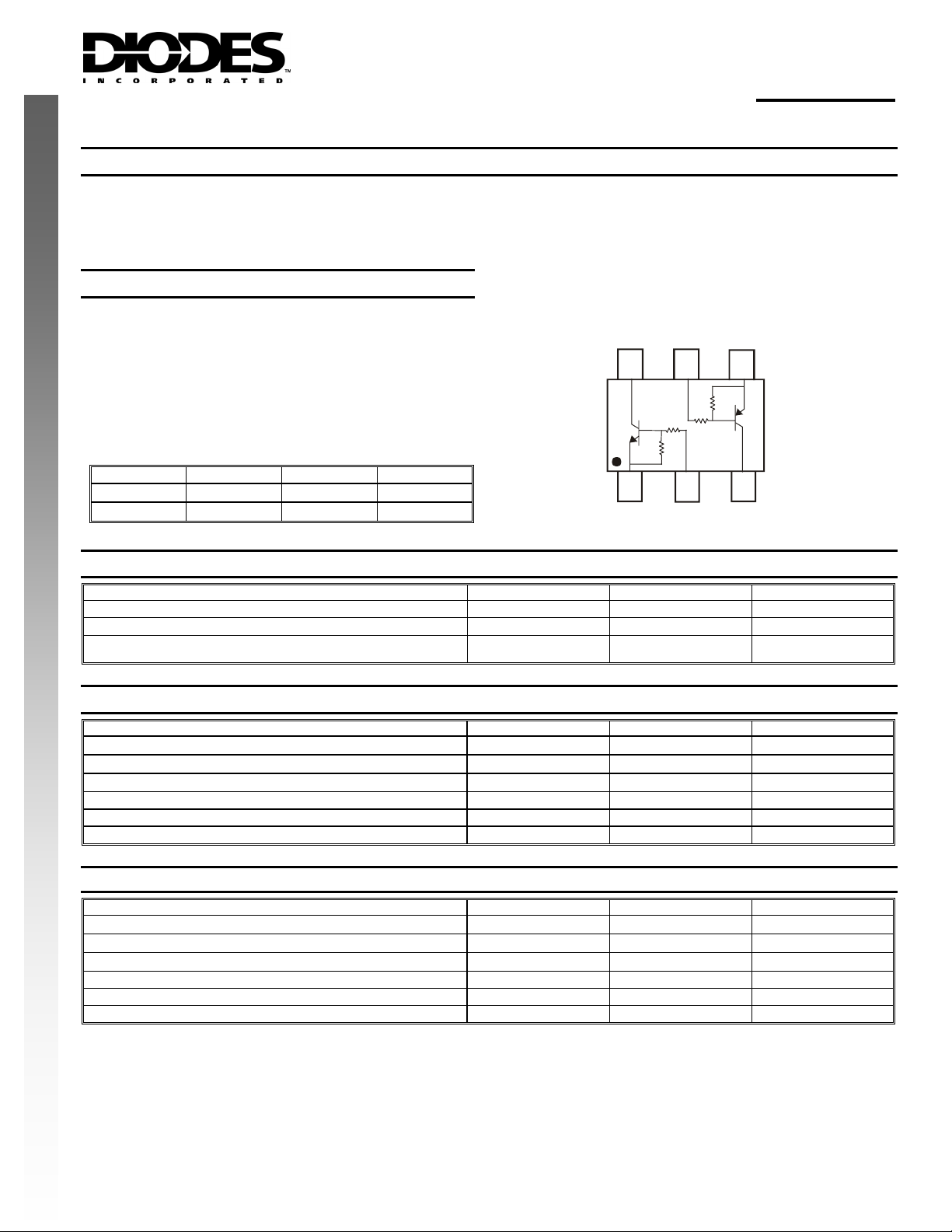
Reference Device Type R1(Nom) R2(Nom)
Q
1
Q
2
NPN 47kΩ 47kΩ
PNP 2.2 kΩ 47kΩ
DEMD48
DUAL NPN/PNP PRE-BIASED TRANSISTOR
SOT-563
6
Q
1
54
R
2
R
1
R
1
2.2k
47k
R
47k
2
47k
Q
2
312
Maximum Ratings, Total Device @T
= 25°C unless otherwise specified
A
Characteristic Symbol Value Unit
Power Dissipation (Note 3)
Thermal Resistance, Junction to Ambient Air (Note 3)
Operating and Storage Temperature Range
P
D
R
JA
θ
T
, T
j
STG
Maximum Ratings, Pre-Biased NPN Transistor, Q1 @T
Characteristic Symbol Value Unit
Collector-Base Voltage
Collector-Emitter Voltage
Emitter-Base Voltage
Input Voltage
Output Current (DC)
Peak Collector Current
V
CBO
V
CEO
V
EBO
V
IN
I
O
I
CM
Maximum Ratings, Pre-Biased PNP Transistor, Q2 @T
Characteristic Symbol Value Unit
Collector-Base Voltage
Collector-Emitter Voltage
Emitter-Base Voltage
Input Voltage
Output Current (DC)
Peak Collector Current
Notes: 1. No purposefully added lead.
2. Diodes Inc.'s "Green" policy can be found on our website at http://www.diodes.com/products/lead_free/index.php.
3. Device mounted on FR-4 PCB; pad layout as shown on Diodes Inc. suggested pad layout document AP02001, which can be found on our website at
http://www.diodes.com/datasheets/ap02001.pdf.
V
CBO
V
CEO
V
EBO
V
IN
I
O
I
CM
DS31224 Rev. 4 - 2
1 of 4
www.diodes.com
300 mW
417 °C/W
-55 to +150 °C
= 25°C unless otherwise specified
A
50 V
50 V
10 V
-10 to +40 V
100 mA
100 mA
= 25°C unless otherwise specified
A
-50 V
-50 V
-10 V
-12 to +5 V
-100 mA
-100 mA
DEMD48
© Diodes Incorporated
Page 2

Electrical Characteristics, Pre-Biased NPN Transistor, Q1 @T
Characteristic Symbol Min Typ Max Unit Test Condition
Collector-Base Cut-Off Current I
Collector-Emitter Cut-Off Current I
Emitter-Base Cut-Off Current I
Input Voltage
Collector-Emitter Saturation Voltage V
CBO
CEO
EBO
V
I(off)
V
I(on)
CE(SAT)
DC Current Gain h
Input Resistance R
Resistance Ratio R2/R
Collector Capacitance C
FE
1
1
C
- - 100 nA VCB = 50V, IE = 0A
- -
- - 90
- 1.2 0.8 V
3 1.6 - V VCE = 0.3V, IO = 2mA
- - 0.15 V IC/IB = 10mA/0.5mA
80 - - - VCE = 5V, IC = 5mA
33 47 61 kΩ -
0.8 1 1.2 - -
- - 2.5 pF VCB = 10V, IE = 0, f = 1MHz
Electrical Characteristics, Pre-Biased PNP Transistor, Q2 @T
NEW PRODUCT
Collector-Base Cut-Off Current I
Collector-Emitter Cut-Off Current I
Emitter-Base Cut-Off Current I
Input Voltage
Collector-Emitter Saturation Voltage V
DC Current Gain h
Input Resistance R
Resistance Ratio R2/R
Collector Capacitance C
1,000
Characteristic Symbol Min Typ Max Unit Test Condition
CBO
CEO
EBO
V
I(off)
V
I(on)
CE(SAT)
FE
1
C
1
- - -100 nA VCB = -50V, IE = 0A
- -
- - -180
- -0.6 -0.5 V
-1.1 -0.75 - V VO = -0.3V, IO = -5mA
- - -0.1 V IC/IB = -5mA/-0.25mA B
100 - - - VCE = -5V, IC = -10mA
1.54 2.2 2.86 kΩ 17 21 26 - -
- - 3.0 pF VCB = -10V, IE = 0, f = 1MHz
= 25°C unless otherwise specified
A
50
1
μA
μA
= 30V, IB = 0A B
V
CE
= 30V, IB = 0A, TB
V
CE
VEB = 5V, IC = 0A
= 150°C
A
VCE = 5V, IO = 100μA
B
= 25°C unless otherwise specified
A
-1
-50
μA
μA
= -30V, IB = 0A B
V
CE
V
= -30V, IB = 0A, TB
CE
VEB = -5V, IC = 0A
= -5V, IO = -100μA
V
CC
= 150°C
A
100
10
1
DS31224 Rev. 4 - 2
2 of 4
www.diodes.com
DEMD48
© Diodes Incorporated
Page 3

NEW PRODUCT
1,000
100
10
1
0.1
1
0.01
DS31224 Rev. 4 - 2
3 of 4
www.diodes.com
DEMD48
© Diodes Incorporated
Page 4

Ordering Information (Note 4)
Device
DEMD48-7
Note: 4. For packaging details, go to our website at http://www.diodes.com/datasheets/ap02007.pdf.
Packaging Shipping
SOT-563 3000/Tape & Reel
Marking Information
D48 YM
2008 2009 2010 2011 2012
V W X Y Z
NEW PRODUCT
Date Code Key
Year 2007
Code U
Month Jan Feb Mar Apr May Jun Jul
Code 1 2 3 4 5 6 7
D48 = Product Type Marking Code
YM = Date Code Marking
Y = Year ex: U = 2007
M = Month ex: 9 = September
Aug Sep Oct Nov Dec
8 9 O N D
Package Outline Dimensions
A
Dim Min Max Typ
B
C
D
G
Diodes Incorporated and its subsidiaries reserve the right to make modifications, enhancements, improvements, corrections or other changes
without further notice to any product herein. Diodes Incorporated does not assume any liability arising out of the application or use of any product
described herein; neither does it convey any license under its patent rights, nor the rights of others. The user of products in such applications shall
assume all risks of such use and will agree to hold Diodes Incorporated and all the companies whose products are represented on our website,
harmless against all damages.
Diodes Incorporated products are not authorized for use as critical components in life support devices or systems without the expressed written
approval of the President of Diodes Incorporated.
K
H
L
M
IMPORTANT NOTICE
LIFE SUPPORT
SOT-563
A 0.15 0.30 0.20
B 1.10 1.25 1.20
C 1.55 1.70 1.60
D - - 0.50
G 0.90 1.10 1.00
H 1.50 1.70 1.60
K 0.55 0.60 0.60
L 0.10 0.30 0.20
M 0.10 0.18 0.11
All Dimensions in mm
DS31224 Rev. 4 - 2
4 of 4
www.diodes.com
DEMD48
© Diodes Incorporated
 Loading...