

Page 1
θ
Please click here to visit our online spice models database.
Features
• Very Sharp Breakdown Characteristics
• Very Tight Tolerance on V
• Ideally Suited for Automated Assembly Processes
• Very Low Leakage Current
• Lead Free By Design/RoHS Compliant (Note 1)
• “Green” Device (Note 2)
Maximum Ratings @T
Forward Voltage @ IF = 10mA VF
Z
= 25°C unless otherwise specified
A
Characteristic Symbol Value Unit
Mechanical Data
• Case: SOD-323
• Case Material: Molded Plastic, “Green” Molding Compound. UL
• Moisture Sensitivity: Level 1 per J-STD-020
• Terminals: Finish - Matte Tin annealed over Alloy 42 leadframe.
• Polarity: Cathode Band
• Marking Information: See Page 6
• Ordering Information: See Page 6
• Weight: 0.004 grams (approximate)
Top View
DDZ9689S - DDZ9717S
SURFACE MOUNT PRECISION ZENER DIODE
Flammability Classification Rating 94V-0
Solderable per MIL-STD-202, Method 208
0.9 V
Thermal Characteristics
Characteristic Symbol Value Unit
Power Dissipation (Note 3)
Thermal Resistance, Junction to Ambient Air (Note 3)
Operating and Storage Temperature Range
Notes: 1. No purposefully added lead.
2. Diode’s Inc.’s “Green” policy can be found on our website at http://www.diodes.com/products/lead_free/index.php.
DDZ9689S - DDZ9717S
Document number: DS30409 Rev. 6 - 2
3.
Device mounted on FR-4 PC board with recommended pad layout, which can be found on our website at
http://www.diodes.com/datasheets/ap02001.pdf.
PD
R
JA
T
J, TSTG
1 of 7
www.diodes.com
200 mW
625
-65 to +150
°C/W
°C
August 2009
© Diodes Incorporated
Page 2
μ
P
P
O
R
PAT
O
N
NSTAN
TAN
O
U
FOR
R
C
URREN
T
DDZ9689S - DDZ9717S
Electrical Characteristics @T
Type
Number
Type
Code
= 25°C unless otherwise specified
A
Zener Voltage Range (Note 3)
VZ @ IZT IZT IR @ VR
Nom (V) Min (V) Max (V)
Maximum Reverse
Leakage Current (Note 4)
A μA
DDZ9689S HH 5.1 4.85 5.36 50 5 3
DDZ9690S HJ 5.6 5.32 5.88 50 2 4
DDZ9691S HK 6.2 5.89 6.51 50 1 5
DDZ9692S HL 6.8 6.46 7.14 50 0.1 5.1
DDZ9693S HM 7.5 7.13 7.88 50 0.1 5.7
DDZ9694S HN 8.2 7.79 8.61 50 0.1 6.2
DDZ9696S HP 9.1 8.65 9.56 50 0.1 6.9
DDZ9697S HQ 10 9.50 10.50 50 0.1 7.6
DDZ9698S HR 11 10.45 11.55 50 0.05 8.4
DDZ9699S HS 12 11.40 12.60 50 0.05 9.1
DDZ9700S HT 13 12.35 13.65 50 0.05 9.8
DDZ9701S HU 14 13.30 14.70 50 0.05 10.6
DDZ9702S HV 15 14.25 15.75 50 0.05 11.4
DDZ9703S HW 16 15.20 16.80 50 0.05 12.1
DDZ9705S (Note 5) HY 18 17.10 18.90 50 0.05 13.6
DDZ9707S MD 20 19.00 21.00 50 0.05 15.2
DDZ9708S ME 22 20.90 23.10 50 0.05 16.7
DDZ9709S MF 24 22.80 25.20 50 0.05 18.2
DDZ9711S MH 27 25.65 28.35 50 0.05 20.4
DDZ9712S MJ 28 26.60 29.40 50 0.05 21.2
DDZ9713S MK 30 28.50 31.50 50 0.05 22.8
DDZ9714S ML 33 31.35 34.65 50 0.05 25.0
DDZ9715S MM 36 34.20 37.80 50 0.05 27.3
DDZ9716S MN 39 37.05 40.95 50 0.05 29.6
DDZ9717S MO 43 40.85 45.15 50 0.05 32.6
Notes: 3. Nominal Zener voltage is measured with the device junction in thermal equilibrium at TT = 30°C ±1°C.
4. Short duration pulse test used to minimize self-heating effect.
5. Qualified to AEC-Q101 Standards for High Reliability
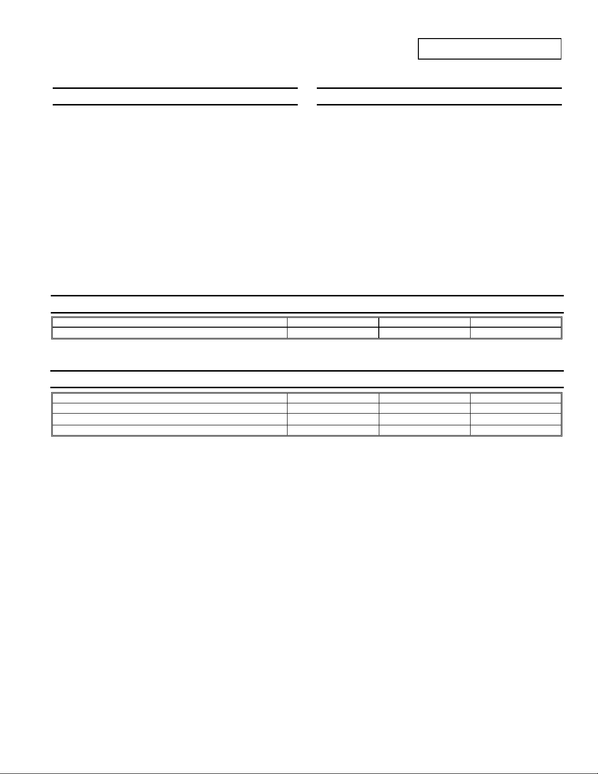
240
1,000
V
(mA)
(mW)
160
I
120
DISSI
WE
,
D
200
80
40
0
250 50 75 100 125 150
T , AMBIENT TEMPERATURE ( C)
A
Fig. 1 Power Derating Curve
°
D
WA
S
E
F
I, I
100
10
1.0
0.1
0.01
0
V , INSTANTANEOUS FORWARD VOLTAGE (V)
F
Fig. 2 Typical Forward C haracter istics
0.2
0.4
0.6 0.8
1.0
1.2
DDZ9689S - DDZ9717S
Document number: DS30409 Rev. 6 - 2
2 of 7
www.diodes.com
August 2009
© Diodes Incorporated
Page 3
R CUR
R
T
NER CUR
REN
T
R CUR
RENT
R CUR
R
T
R
C
U
R
RENT
DDZ9689S - DDZ9717S
100m
10m
1m
(A)
EN
Z
I, ZENE
100n
10n
35
40 45
100m
10m
05
10 15
20
25 30
100m
10m
(A)
1m
Z
I, ZE
100n
3.0 5.0 7.0
4.0 6.0 8.0
V , ZENER VOLTAGE (V)
Z
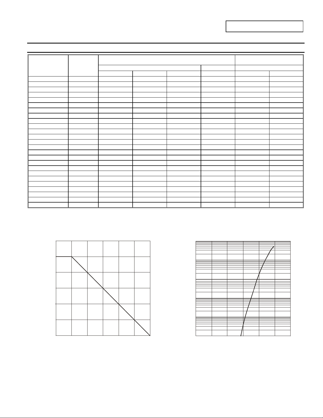
Fig. 4 Typical Zener Breakdown Cha r ac t eristics,
DDZ9692S - DDZ9694S
100m
10m
(A)
1m
EN
9.0
(A)
1m
Z
I, ZENE
100n
10.0
8.0 11.0 13.0 15.0
V , ZENER VOLTAGE (V)
Fig. 5 Typical Zener Br eakdown Characteristics,
Z
DDZ9696S - DDZ9701S
12.0 14.0
100m
10m
(A)
1m
Z
I, ZENE
100n
14 16
15 17
V , ZENER VOLT AGE (V)
Z
18 20
19
Fig. 6 Typical Zener Breakdown Characteristics,
DDZ9702S - DDZ9705S
Z
I, ZENE
100n
19 21 23
20
V , ZENER VOLTAGE (V)
Z
Fig. 7 Typical Zener Breakdown Characte r istics,
DDZ9707S - DDZ9709S
22
24
25
DDZ9689S - DDZ9717S
Document number: DS30409 Rev. 6 - 2
3 of 7
www.diodes.com
August 2009
© Diodes Incorporated
Page 4

R
CUR
RENT
NER CUR
REN
T
DDZ9689S - DDZ9717S
100m
10m
(A)
1m
100m
10m
(A)
1m
Z
I, ZENE
100n
26 30 34 38
28
V , ZENER VOLTAGE (V)
Z
32
Fig. 8 Typical Zener Breakdown Cha r ac t eristics,
DDZ9711S - DDZ9715S
100
V =1V
R
36
T = 25 °C
J
f = 1MHz
Z
I, ZE
100n
10,000
1,000
38
42
40 44
V , ZENER VOLTAGE (V)
Z
46
48
Fig. 9 Typical Zen er B r ea kdown Cha r acteristics ,
DDZ9716S - DDZ9717S
50
V = 2V
R
10
T
C , TOTAL CAP ACITANCE (pF)
1
10
V , NOMINAL ZENER VOLTAGE (V)
Z
Fig. 10 Total Capacitance vs. Nominal Zener Voltage
10,000
1,000
100
10
100
10
1
0.1
1001
2
3
Fig. 11 Typical Zener Imp edance Characteristi cs,
4
V , ZENER VOLT AGE (V)
Z
5
DDZ9689S - DDZ9692S
67
10,000
1,000
100
10
1
0.1
78
9
V , ZENER VOLTAGE (V)
Z
10 11 12
Fig. 12 Typical Zener Impedance Characteristics,
DDZ9693S - DDZ9699S
1
0.1
12
13 14
V , ZENER VOLTAGE (V)
Z
15
16
Fig. 13 Typical Zener Impe dance Characteristics,
DDZ9699S - DDZ9705S
17
18
DDZ9689S - DDZ9717S
Document number: DS30409 Rev. 6 - 2
4 of 7
www.diodes.com
August 2009
© Diodes Incorporated
Page 5

T
C
TEMPERATURE C
OEF
FIC
T
T
C
TEMP
R
TUR
C
OEF
F
CIEN
T
T
C
TEMPER
TUR
C
O
F
FIC
T
DDZ9689S - DDZ9717S
10,000
1,000
100
10
0.1
10,000
1
18
19 20
V , ZENER VOLT AGE (V)
Z
21
22
23
Fig. 14 Typical Zener Impe dance Char act eristics,
DDZ970 5S - DDZ9 709S
24
10,000
1,000
100
10
1
0.1
24 26 28
Fig. 15 Typical Zener Im pedance Ch ar acteristics,
0.12
V , ZENER VOLTAGE (V)
Z
DDZ9709S - DDZ9714S
30 32 34
0.10
1,000
IEN
0.08
0.06
100
0.04
0.02
10
0
-0.02
Z
1
0.1
34
36 38
V , ZENER VOLTAGE (V)
Z
40
42
44 4846
Fig. 16 Typical Zener Im pedance Characteristics,
DDZ9715S - DDZ9716S
0.12
0.10
0.08
I
0.06
0.04
E
0.02
A
E
0
-0.02
Z
OF ZENER VOLTAGE (% /°C)
-0.04
of V ,
-0.06
-0.08
10
12
14
V , ZENER VOLT AGE (V)
Z
16 20
18
Fig. 18 Typical Temperature Coefficient of Zener
Voltage vs . Z ener Voltag e, D DZ 9697S - DDZ9707S
DDZ9689S - DDZ9717S
Document number: DS30409 Rev. 6 - 2
5 of 7
www.diodes.com
OF ZENER VOLTAGE ( %/ °C)
-0.04
of V ,
-0.06
-0.08
0610
42
V , ZENER VOLTAGE (V )
Z
8
Fig. 17 Typical Temperature Coefficient of Zener
Voltage vs . Z ener Voltage , DD Z9692S - D DZ9697S
0.12
0.10
IEN
0.08
0.06
E
0.04
E
0.02
A
0
-0.02
Z
OF ZENER VOLTAGE (%/°C)
-0.04
of V ,
-0.06
-0.08
20
22
24
V , ZENER VOLTAGE (V)
Z
26 30
28
Fig. 19 Typical Temperature Coefficient of Zene r
Voltage vs . Z ener Voltage, DDZ9707S - D DZ9713S
August 2009
© Diodes Incorporated
Page 6

T
C
TEMPERATURE C
O
F
FIC
T
0.12
0.10
IEN
0.08
0.06
E
0.04
0.02
0
-0.02
Z
OF ZENER VOLTAG E (%/ °C)
-0.04
of V ,
-0.06
-0.08
30
Voltage vs . Z ener Voltage , DD Z9713S - D DZ9716S
34
Fig. 20 Typical Temperature Coefficient of Zener
38
V , ZENER VOLTAGE (V )
Z
42 50
46
DDZ9689S - DDZ9717S
Ordering Information (Note 6)
Part Number Case Packaging
(Type Number)-7* SOD-323 3000/Tape & Reel
*Example: The part number for the 6.2 Volt device would be DDZ9691S-7.
Notes: 6. For packaging details, go to our website at http://www.diodes.com/datasheets/ap02007.pdf.
Marking Information
XX
xx = Product Type Marking Code
(See Electrical Characteristics Table)
Package Outline Dimensions
DDZ9689S - DDZ9717S
Document number: DS30409 Rev. 6 - 2
BA
M
C
H
K
L
J
6 of 7
www.diodes.com
SOD-323
Dim Min Max
A 0.25 0.35
B 1.20 1.40
C 2.30 2.70
H 1.60 1.80
J 0.00 0.10
K 1.0 1.1
L 0.20 0.40
M 0.10 0.15
α
All Dimensions in mm
0° 8°
August 2009
© Diodes Incorporated
Page 7

DDZ9689S - DDZ9717S
Suggested Pad Layout
DIODES INCORPORATED MAKES NO WARRANTY OF ANY KIND, EXPRESS OR IMPLIED, WITH REGARDS TO THIS DOCUMENT,
INCLUDING, BUT NOT LIMITED TO, THE IMPLIED WARRANTIES OF MERCHANTABILITY AND FITNESS FOR A PARTICULAR PURPOSE
(AND THEIR EQUIVALENTS UNDER THE LAWS OF ANY JURISDICTION).
Diodes Incorporated and its subsidiaries reserve the right to make modifications, enhancements, improvements, corrections or other changes
without further notice to this document and any product described herein. Diodes Incorporated does not assume any liability arising out of the
application or use of this document or any product described herein; neither does Diodes Incorporated convey any license under its patent or
trademark rights, nor the rights of others. Any Customer or user of this document or products described herein in such applications shall assume
all risks of such use and will agree to hold Diodes Incorporated and all the companies whose products are represented on Diodes Incorporated
website, harmless against all damages.
Diodes Incorporated does not warrant or accept any liability whatsoever in respect of any products purchased through unauthorized sales channel.
Should Customers purchase or use Diodes Incorporated products for any unintended or unauthorize d application, Customers shall indemnify and
hold Diodes Incorporated and its representatives harmless against all claims, damages, expenses, and attorney fees arising out of, directly or
indirectly, any claim of personal injury or death associated with such unintended or unauthorized application.
Products described herein may be covered by one or more United States, international or foreign patents pending. Product names and markings
noted herein may also be covered by one or more United States, international or foreign trademarks.
Diodes Incorporated products are specifically not authorized for use as critical components in life support devices or systems without the express
written approval of the Chief Executive Officer of Diodes Incorporated. As used herein:
A. Life support devices or systems are devices or systems which:
1. are intended to implant into the body, or
2. support or sustain life and whose failure to perform when properly used in accordance with instructions for use provided in the
labeling can be reasonably expected to result in significant injury to the user.
B. A critical component is any component in a life support device or system whose failure to perform can be reasonably expected to cause the
failure of the life support device or to affect its safety or effectiveness.
Customers represent that they have all necessary expertise in the safety and regulatory ramifications of their life support devices or systems, and
acknowledge and agree that they are solely responsible for all legal, regulatory and safety-related requirements concerning their products and any
use of Diodes Incorporated products in such safety-critical, life support devices or systems, notwithstanding any devices- or systems-related
information or support that may be provided by Diodes Incorporated. Further, Customers must fully indemnify Diodes Incorporated and its
representatives against any damages arising out of the use of Diodes Incorporated products in such safety-critical, life support devices or systems.
Copyright © 2009, Diodes Incorporated
www.diodes.com
X
Y
C
Dimensions Value (in mm)
Z 3.75
G 1.05
X 0.65
Y 1.35
C 2.40
G
Z
IMPORTANT NOTICE
LIFE SUPPORT
DDZ9689S - DDZ9717S
Document number: DS30409 Rev. 6 - 2
7 of 7
www.diodes.com
August 2009
© Diodes Incorporated
 Loading...