

Page 1
Features
• 500mW Power Dissipation on Ceramic PCB
• Specified at a Low Test Current (50µA), ideal for low bias and
portable battery-powered applications
• Ideally Suited for Automated Assembly Processes
• Totally Lead-Free & Fully RoHS Compliant (Notes 1 & 2)
• Halogen and Antimony Free. “Green” Device (Note 3)
DDZ9678 - DDZ9717
SURFACE MOUNT LOW CURRENT ZENER DIODE
Mechanical Data
• Case: SOD123
• Case Material: Molded Plastic. UL Flammability Classification
Rating 94V-0
• Moisture Sensitivity: Level 1 per J-STD-020
• Terminal Connections: Cathode Band
• Terminals: Finish - Matte Tin annealed over Alloy 42 leadframe.
Solderable per MIL-STD-202, Method 208
• Weight: 0.01 grams (approximate)
SOD123
Top View
e3
Ordering Information (Notes 4 & 5)
Part Number Compliance Case Packaging
(Type Number)-7* Standard SOD123 3000/Tape & Reel
(Type Number)Q-7* (Note 6) Automotive SOD123 3000/Tape & Reel
*Example: The part number for the commercial grade 4.7 Volt device would be DDZ9688-7 and the part number for the automotive grade 4.7 Volt device would be
DDZ9688Q-7.
Notes: 1. No purposely added lead. Fully EU Directive 2002/95/EC (RoHS) & 2011/65/EU (RoHS 2) compliant.
2. See http://www.diodes.com/quality/lead_free.html for more information about Diodes Incorporated’s definitions of Halogen- and Antimony-free, "Green"
and Lead-free.
3. Halogen- and Antimony-free "Green” products are defined as those which contain <900ppm bromine, <900ppm chlorine (<1500ppm total Br + Cl) and
<1000ppm antimony compounds.
4. Product manufactured with Date Code V9 (week 33, 2008) and newer are built with Green Molding Compound. Product manufactured prior to Date
Code V9 are built with Non-Green Molding Compound and may contain Halogens or Sb2O3 Fire Retardants.
5. For packaging details, go to our website at http://www.diodes.com/products/packages.html.
6. Only products denoted Note 10 in the "Electrical Characteristics" table are currently available as automotive grade devices.
Marking Information
Date Code Key
Year 2006 2007 2008 2009 2010 2011 2012 2013 2014 2015 2016 2017
Code T U V W X Y Z A B C D E
Month Jan Feb Mar Apr May Jun Jul Aug Sep Oct Nov Dec
Code 1 2 3 4 5 6 7 8 9 O N D
DDZ9678 - DDZ9717
Document number: DS30410 Rev. 15 - 2
xx
YM
www.diodes.com
xx = Product Type Marking Code -
(See Electrical Characteristics Table)
YM = Date Code Marking
Y = Year (ex: T = 2006)
M = Month (ex: 9 = September)
1 of 7
November 2013
© Diodes Incorporated
Page 2
DDZ9678 - DDZ9717
Maximum Ratings (@T
= +25°C, unless otherwise specified.)
A
Characteristic Symbol Value Unit
Forward Voltage @ IF = 10mA VF
0.9 V
Thermal Characteristics
Characteristic Symbol Value Unit
Power Dissipation (Note 7)
Thermal Resistance, Junction to Ambient Air (Note 7)
Operating and Storage Temperature Range
P
R
T
J, TSTG
θJA
D
500 mW
305 °C/W
-65 to +150 °C
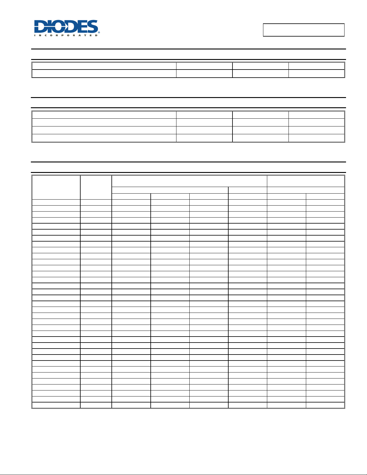
Electrical Characteristics (@T
Type
Number
Type
Code
= +25°C, unless otherwise specified.)
A
Zener Voltage Range (Note 8)
VZ @ IZT I
Maximum Reverse
Leakage Current (Note 9)
I
ZT
@ VR
R
Nom (V) Min (V) Max (V) µA µA V
DDZ9678 D1 1.8 1.71 1.89 50 7.5 1
DDZ9681 (Note 10) H9 2.4 2.28 2.52 50 2 1
DDZ9682 (Note 10) HA 2.7 2.565 2.835 50 1 1
DDZ9683 HB 3.0 2.85 3.15 50 0.8 1
DDZ9684 (Note 10) HC 3.3 3.13 3.47 50 7.5 1.5
DDZ9685 (Note 10) HD 3.6 3.42 3.78 50 7.5 2
DDZ9686 (Note 10) HE 3.9 3.70 4.10 50 5 2
DDZ9687 (Note 10) HF 4.3 4.09 4.52 50 4 2
DDZ9688 (Note 10) HG 4.7 4.47 4.94 50 5 3
DDZ9689 (Note 10) HH 5.1 4.85 5.36 50 5 3
DDZ9690 (Note 10) HJ 5.6 5.32 5.88 50 2 4
DDZ9691 HK 6.2 5.89 6.51 50 1 5
DDZ9692 HL 6.8 6.46 7.14 50 0.1 5.1
DDZ9693 (Note 10) HM 7.5 7.13 7.88 50 0.1 5.7
DDZ9694 (Note 10) HN 8.2 7.79 8.61 50 0.1 6.2
DDZ9696 (Note 10) HP 9.1 8.65 9.56 50 0.1 6.9
DDZ9697 (Note 10) HQ 10 9.50 10.50 50 0.1 7.6
DDZ9698 HR 11 10.45 11.55 50 0.05 8.4
DDZ9699 (Note 10) HS 12 11.40 12.60 50 0.05 9.1
DDZ9700 (Note 10) HT 13 12.35 13.65 50 0.05 9.8
DDZ9701 (Note 10) HU 14 13.30 14.70 50 0.05 10.6
DDZ9702 HV 15 14.25 15.75 50 0.05 11.4
DDZ9703 HW 16 15.20 16.80 50 0.05 12.1
DDZ9704 (Note 10) H8 17 16.15 17.85 50 0.05 12.9
DDZ9705 HY 18 17.10 18.90 50 0.05 13.6
DDZ9707 MD 20 19.00 21.00 50 0.05 15.2
DDZ9708 ME 22 20.90 23.10 50 0.05 16.7
DDZ9709 MF 24 22.80 25.20 50 0.05 18.2
DDZ9711 MH 27 25.65 28.35 50 0.05 20.4
DDZ9712 MJ 28 26.60 29.40 50 0.05 21.2
DDZ9713 MK 30 28.50 31.50 50 0.05 22.8
DDZ9714 ML 33 31.35 34.65 50 0.05 25.0
DDZ9715 MM 36 34.20 37.80 50 0.05 27.3
DDZ9716 MN 39 37.05 40.95 50 0.05 29.6
DDZ9717 MO 43 40.85 45.15 50 0.05 32.6
Notes: 7. Device mounted on ceramic PCB = 7.6mm x 9.4mm x 0.87mm with pad areas 25mm2 at TA = +25°C or mounted on FR-5 = 3.5x1.5 inches with
recommended pad layout, which can be found on our website at http://www.diodes.com, at T
8. Nominal Zener voltage is measured with the device junction in thermal equilibrium at T
9. Short duration pulse test used to minimize self-heating effect.
10. Qualified to AEC-Q101 Standards for High Reliability. Please contact the Diodes, Inc. sales department for assistance in ordering any products
expected to meet automotive requirements.
DDZ9678 - DDZ9717
Document number: DS30410 Rev. 15 - 2
2 of 7
www.diodes.com
= +75°C.
L
= +30°C ±1°C.
T
November 2013
© Diodes Incorporated
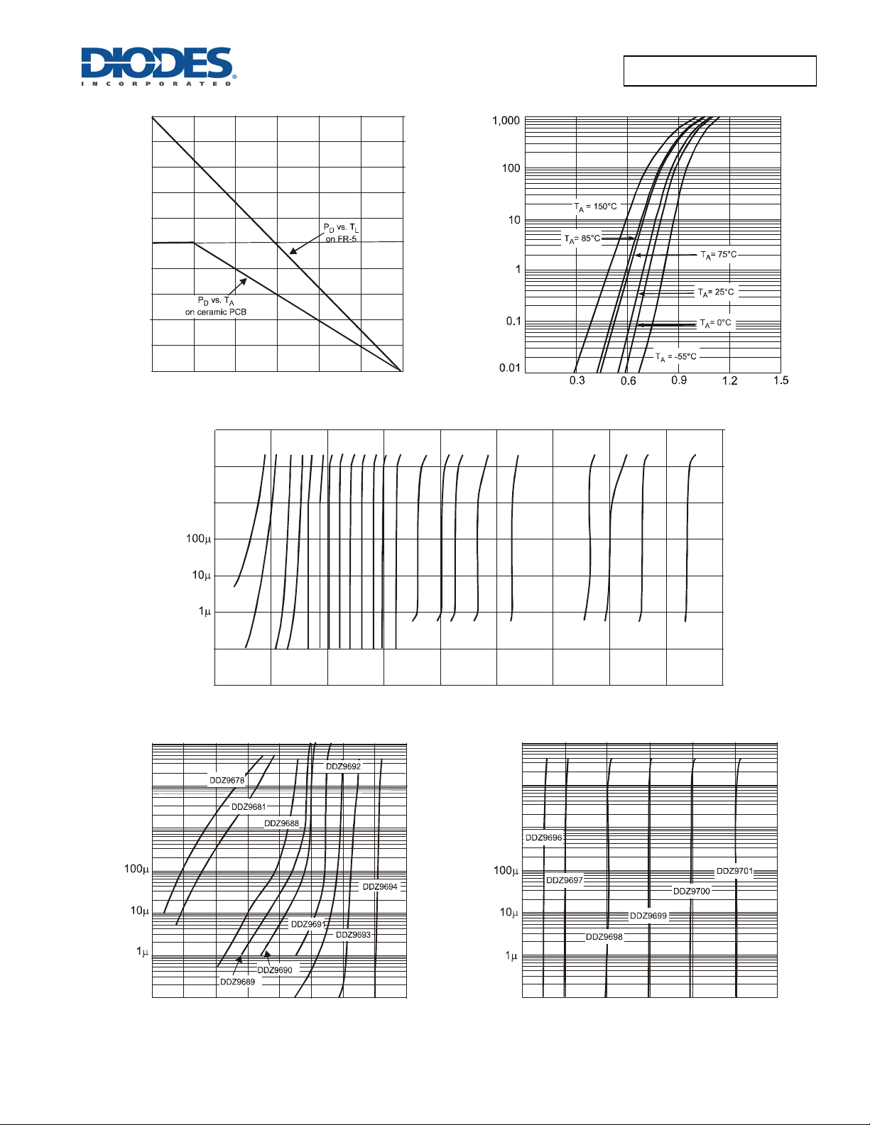
Page 3
P, P
OWER
PATIO
O
U
O
RWARD C
URR
R CUR
RENT
R C
U
R
RENT
N
R C
URR
N
T
DDZ9678 - DDZ9717
1.0
0.9
0.8
N (W)
0.7
ENT (mA)
0.6
0.5
DISSI
0.4
S F
0.3
D
0.2
0.1
0
2505075100125
T , AMBIENT TEMPERATURE ( C)
A
Fig. 1 Power Derating Curve
150
°
F
I , INSTANTANE
0
V , INSTANTANEOUS FORWARD VOLTAGE (V)
F
Fig. 2 Typical Forward C haracteristics
100m
9681
9688
9692
9693
9694
9696
9697
9698
9699
9700
9701
9702
9703
9705
9707
9708
9709
9711
9714
9715
9716
9717
10m
100m
10m
(A)
1m
1m
(A)
Z
I, ZENE
100n
10n
05
10 15
20
V , ZENER VOLTAGE (V)
Z
25 30 35
Fig. 3 Typical Zener Breakdown Characteristics
100m
10m
(A)
1m
E
E
40
45
Z
I, ZENE
100n
2.0 3.0 4.0 5.0 6.0
1.0
V , ZENER VOLTAGE (V)
Z
7.0 8.0
Fig. 4 Typical Zener Breakdown Characteristics,
DDZ9678 - DDZ9694
9.0
Z
I, ZE
100n
10.0
8.0 11.0 13.0 15.0
V , ZENER VOLTAGE (V)
Z
12.0 14.0
Fig. 5 Typical Zener Breakdown Characteristics,
DDZ9696 - DDZ9701
DDZ9678 - DDZ9717
Document number: DS30410 Rev. 15 - 2
3 of 7
www.diodes.com
November 2013
© Diodes Incorporated
Page 4

R C
U
R
R
T
NER CUR
R
N
T
NER CUR
REN
T
R CUR
RENT
DDZ9678 - DDZ9717
100m
10m
(A)
1m
EN
Z
I, ZENE
100m
14
15 17 19
16
V , ZENER VOLTAGE (V)
Fig. 6 Typical Characteristics,
Z
Zener Breakdown
18 20
DDZ9702 - DDZ9705
100m
10m
(A)
1m
E
Z
I, ZE
19 21 23
20
V , ZENER VOLTAGE (V)
Fig. 7 Typical Characteristics,
Z
Zener Breakdown
DDZ9707 - DDZ9709
100m
22
24
25
10m
(A)
1m
Z
I, ZE
26 30
28 32 36
V , ZENER VOLTAGE (V)
Z
Fig. 8 Typical Characteristics,
Zener B reakdown
DDZ9711 - DDZ9715
100
V =1V
R
V = 2V
R
10
34
T= 25 °C
J
f = 1MHz
38
10m
(A)
1m
Z
I, ZENE
38
42
40 44
V , ZENER VOLTAGE (V)
Z
Fig. 9 Typical Zener Breakdown Characteristics,
DDZ9716 - DDZ9717
10,000
1,000
100
46
48
50
10
T
C , TOTAL CAPACITANCE (pF)
1
V , NOMINAL ZENER VOLTAGE (V)
Fig. 10 Total Capacitance vs. Nominal Zener Voltage
Z
10
1001
1
0.1
2
3
4
V , ZENER VOLTAGE (V)
Z
5
Fig. 11 Typical Zener Impedance Characteristics,
6
7
DDZ9681 - DDZ9692
DDZ9678 - DDZ9717
Document number: DS30410 Rev. 15 - 2
4 of 7
www.diodes.com
November 2013
© Diodes Incorporated
Page 5

T
C
TEMP
R
TUR
C
O
F
F
C
T
DDZ9678 - DDZ9717
10,000
1,000
100
10
0.1
10,000
1
7
8
9
V , ZENER VOLTAGE (V)
Z
10
11 12
Fig. 12 Typical Zener Impedance Characteristics,
DDZ9693 - DDZ9699
10,000
1,000
100
10
0.1
10,000
1
12
13 14
V , ZENER VOLTAGE (V)
Z
15
16
17
Fig. 13 Typical Zener Impedance Characteristics,
DDZ9699 - DDZ9705
18
1,000
100
10
0.1
10,000
1
18
19 20
V , ZENER VOLTAGE (V)
Z
21
22
23
Fig. 14 Typical Zener Impedance Characteristics,
DDZ9705 - DDZ9709
24
1,000
100
10
1
0.1
24 26 28
V , ZENER VOLTAGE (V)
Z
30 32 34
Fig. 15 Typical Zener Impedance Characteristics,
DDZ9709 - DDZ9714
0.12
0.10
1,000
100
10
IEN
0.08
I
0.06
E
0.04
E
0.02
A
E
0
-0.02
Z
OF ZENER VOLTAGE (%/°C)
1
0.1
36
38 40
V , ZENER VOLTAGE (V)
Z
42
44
46
48
Fig. 16 Typical Zener Impedance Characteristics,
DDZ9715 - DDZ9717
DDZ9678 - DDZ9717
Document number: DS30410 Rev. 15 - 2
5 of 7
www.diodes.com
-0.04
of V ,
-0.06
-0.08
0610
42
V , ZENER VOLTAGE (V)
Z
Fig. 17 Typical Temperature Coefficient of
Zener Voltage vs. Zener Voltage, DDZ9681 - DDZ9697
8
November 2013
© Diodes Incorporated
Page 6

T
C
TEMP
R
T
U
RE C
OEF
F
C
T
T
C
TEMPERATUR
C
OEF
FIC
T
T
C
TEMPERATURE C
OEF
FIC
T
DDZ9678 - DDZ9717
0.12
0.10
IEN
0.08
I
0.06
0.04
0.02
A
E
0
-0.02
Z
OF ZENER VOLTAGE (%/°C)
-0.04
of V ,
-0.06
-0.08
10
Zener Voltage vs. Zener Voltage, DDZ9697 - DDZ9707
0.12
0.10
IEN
0.08
12
Fig. 18 Typical Temperature Coefficient of
14
V , ZENER VOLTAGE (V)
Z
16 20
18
0.12
0.10
IEN
0.08
0.06
0.04
E
0.02
0
-0.02
Z
OF ZENER VOLTAGE (%/°C)
-0.04
of V ,
-0.06
-0.08
20
Zener Voltage vs. Zener Voltage, DDZ9707 - DDZ9713
22
Fig. 19 Typical Temperature Coefficient of
24
V , ZENER VOLTAGE (V)
Z
26 30
28
0.06
0.04
0.02
0
-0.02
Z
OF ZENER VOLTAGE (%/°C)
-0.04
of V ,
-0.06
-0.08
30
Zener Voltage vs. Zener Voltage, DDZ9713 - DDZ9717
34
Fig. 20 Typical Temperature Coefficient of
38
V , ZENER VOLTAGE (V)
Z
42 50
46
T , AMBIENT TEMPERATURE (°C)
Fig. 21
A
Typical Leakage vs. Ambient Temperature, DDZ9681
Package Outline Dimensions
Please see AP02002 at http://www.diodes.com/datasheets/ap02002.pdf for latest version.
DDZ9678 - DDZ9717
Document number: DS30410 Rev. 15 - 2
B
M
C
H
SOD123
Dim Min Max
A 0.55 Typ
A
B 1.40 1.70
C 3.55 3.85
H 2.55 2.85
J 0.00 0.10
K 1.00 1.35
K
L
6 of 7
www.diodes.com
L 0.25 0.40
M 0.10 0.15
α
0 8°
All Dimensions in mm
November 2013
© Diodes Incorporated
Page 7

DDZ9678 - DDZ9717
Suggested Pad Layout
Please see AP02001 at http://www.diodes.com/datasheets/ap02001.pdf for the latest version.
Y
DIODES INCORPORATED MAKES NO WARRANTY OF ANY KIND, EXPRESS OR IMPLIED, WITH REGARDS TO THIS DOCUMENT,
INCLUDING, BUT NOT LIMITED TO, THE IMPLIED WARRANTIES OF MERCHANTABILITY AND FITNESS FOR A PARTICULAR PURPOSE
(AND THEIR EQUIVALENTS UNDER THE LAWS OF ANY JURISDICTION).
Diodes Incorporated and its subsidiaries reserve the right to make modifications, enhancements, improvements, corrections or other changes
without further notice to this document and any product described herein. Diodes Incorporated does not assume any liability arising out of the
application or use of this document or any product described herein; neither does Diodes Incorporated convey any license under its patent or
trademark rights, nor the rights of others. Any Customer or user of this document or products described herein in such applications shall assume
all risks of such use and will agree to hold Diodes Incorporated and all the companies whose products are represented on Diodes Incorporated
website, harmless against all damages.
Diodes Incorporated does not warrant or accept any liability whatsoever in respect of any products purchased through unauthorized sales channel.
Should Customers purchase or use Diodes Incorporated products for any unintended or unauthorized application, Customers shall indemnify and
hold Diodes Incorporated and its representatives harmless against all claims, damages, expenses, and attorney fees arising out of, directly or
indirectly, any claim of personal injury or death associated with such unintended or unauthorized application.
Products described herein may be covered by one or more United States, international or foreign patents pending. Product names and markings
noted herein may also be covered by one or more United States, international or foreign trademarks.
This document is written in English but may be translated into multiple languages for reference. Only the English version of this document is the
final and determinative format released by Diodes Incorporated.
Diodes Incorporated products are specifically not authorized for use as critical components in life support devices or systems without the express
written approval of the Chief Executive Officer of Diodes Incorporated. As used herein:
A. Life support devices or systems are devices or systems which:
1. are intended to implant into the body, or
labeling can be reasonably expected to result in significant injury to the user.
B. A critical component is any component in a life support device or system whose failure to perform can be reasonably expected to cause the
failure of the life support device or to affect its safety or effectiveness.
Customers represent that they have all necessary expertise in the safety and regulatory ramifications of their life support devices or systems, and
acknowledge and agree that they are solely responsible for all legal, regulatory and safety-related requirements concerning their products and any
use of Diodes Incorporated products in such safety-critical, life support devices or systems, notwithstanding any devices- or systems-related
information or support that may be provided by Diodes Incorporated. Further, Customers must fully indemnify Diodes Incorporated and its
representatives against any damages arising out of the use of Diodes Incorporated products in such safety-critical, life support devices or systems.
Copyright © 2013, Diodes Incorporated
www.diodes.com
2. support or sustain life and whose failure to perform when properly used in accordance with instructions for use provided in the
DDZ9678 - DDZ9717
Document number: DS30410 Rev. 15 - 2
X1
X
G
IMPORTANT NOTICE
LIFE SUPPORT
7 of 7
www.diodes.com
Dimensions Value (in mm)
G 2.250
X 0.900
X1 4.050
Y 0.950
November 2013
© Diodes Incorporated
 Loading...