

Page 1
Features
• Very Tight Tolerance on VZ
• Ideally Suited for Automated Assembly Processes
• Totally Lead-Free & Fully RoHS Compliant (Notes 1 & 2)
• Halogen and Antimony Free. “Green” Device (Notes 3 & 4)
• Qualified to AEC-Q101 Standards for High Reliability
SOD123
Top View
DDZ5V1B - DDZ43
SURFACE MOUNT PRECISION ZENER DIODE
Mechanical Data
• Case: SOD123
• Case Material: Molded Plastic, “Green Molding Compound”.
UL Flammability Classification Rating 94V-0
• Moisture Sensitivity: Level 1 per J-STD-020
• Terminal Connections: Cathode Band
• Terminals: Finish - Matte Tin annealed over Alloy 42
leadframe. Solderable per MIL-STD-202, Method 208
• Weight: 0.01 grams (approximate)
Ordering Information (Notes 4 & 5)
Part Number Qualification Case Packaging
DDZ(VZ Rank)-7* Commercial SOD123 3000/Tape & Reel
DDZ(VZ Rank)Q-7* Automotive SOD123 3000/Tape & Reel
* Example: The part number for the 6.2 Volt device would be DDZ6V2B-7.
Notes: 1. No purposely added lead. Fully EU Directive 2002/95/EC (RoHS) & 2011/65/EU (RoHS 2) compliant.
2. See http://www.diodes.com/quality/lead_free.html for more information about Diodes Incorporated’s definitions of Halogen- and Antimony-free, "Green"
and Lead-free.
3. Halogen- and Antimony-free "Green” products are defined as those which contain <900ppm bromine, <900ppm chlorine (<1500ppm total Br + Cl) and
<1000ppm antimony compounds.
4. Product manufactured with Date Code V9 (week 33, 2008) and newer are built with Green Molding Compound. Product manufactured prior to Date
Code V9 are built with Non-Green Molding Compound and may contain Halogens or Sb2O3 Fire Retardants.
5. For packaging details, go to our website at http://www.diodes.com/products/packages.html.
Marking Information
Date Code Key
Year 2003 2004 … 2011 2012 2013 2014 2015 2016 2017
Code P R … Y Z A B C D E
Month Jan Feb Mar Apr May Jun Jul Aug Sep Oct Nov Dec
Code 1 2 3 4 5 6 7 8 9 O N D
DDZ5V1B - DDZ43
Document number: DS30407 Rev. 13 - 2
xx
YM
www.diodes.com
xx = Product Type Marking Code
(See Electrical Characteristics Table)
YM = Date Code Marking
Y = Year (ex: T = 2006)
M = Month (ex: 9 = September)
1 of 7
December 2013
© Diodes Incorporated
Page 2
θ
K
K
DDZ5V1B - DDZ43
Maximum Ratings (@T
= +25°C, unless otherwise specified.)
A
Characteristic Symbol Value Unit
Forward Voltage @ IF = 10mA VF
0.9 V
Thermal Characteristics
Characteristic Symbol Value Unit
Power Dissipation (Note 6) @TL = +75°C
Power Dissipation (Note 7) @TA = +25°C
Thermal Resistance, Junction to Ambient Air (Note 7)
Operating and Storage Temperature Range
P
P
R
T
J, TSTG
D
D
JA
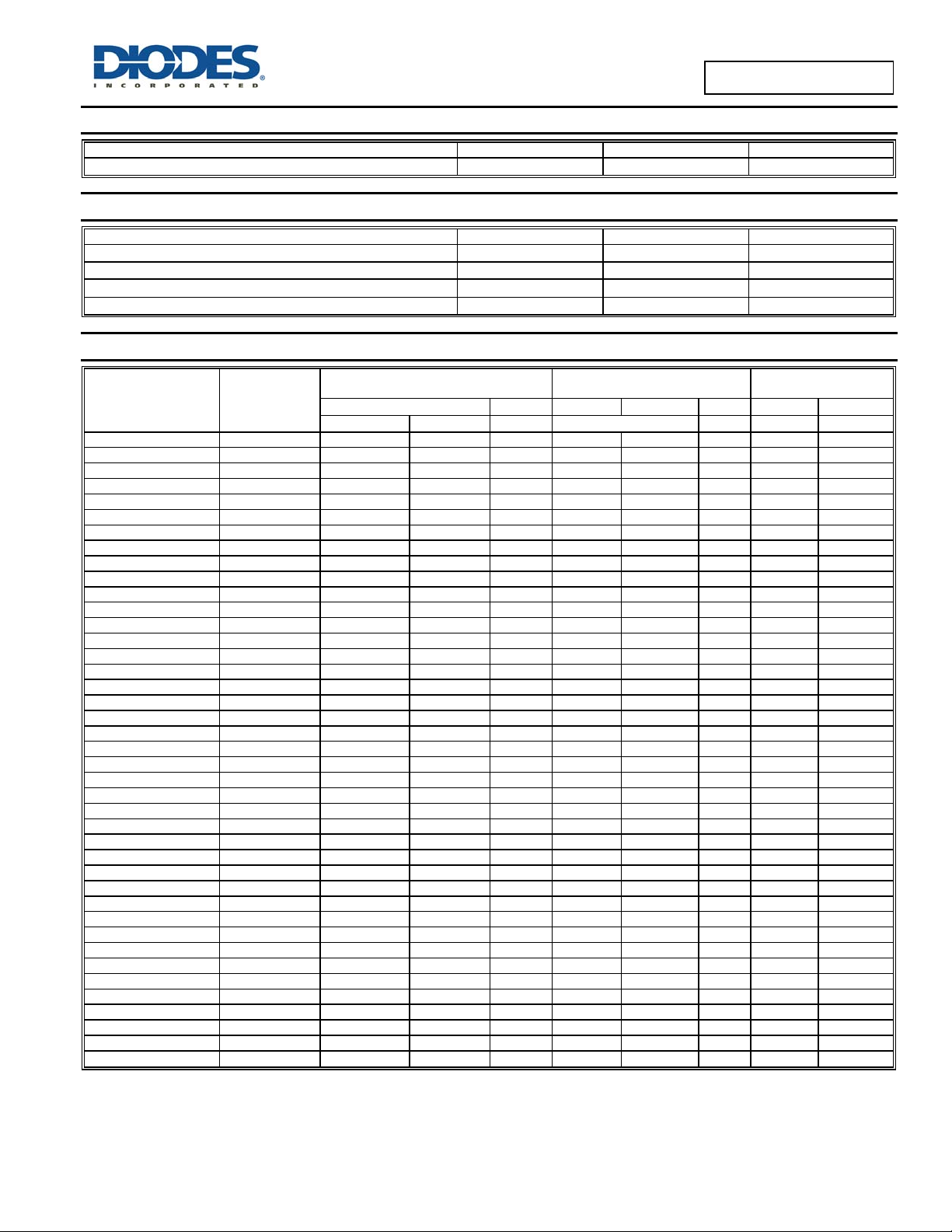
Electrical Characteristics (@T
Type Number Marking Code
= +25°C, unless otherwise specified.)
A
Zener Voltage Range
(Notes 8 & 9)
VZ @ IZT IZT Z
Maximum Zener Impedance
@ IZTZ
ZT
Min (V) Max (V) mA
DDZ5V1B KM 4.94 5.20 20 17 480 1 5 1.5
DDZ5V6B KN 5.45 5.73 20 11 400 1 0.5 2.5
DDZ6V2B KO 5.96 6.27 20 7 150 1 0.5 4.0
DDZ6V8B KP 6.49 6.83 20 5 150 0.5 0.1 5.0
DDZ6V8C YP 6.66 7.01 20 5 150 0.5 0.1 5.0
DDZ7V5B KQ 7.07 7.45 20 6 120 0.5 0.1 6.0
DDZ7V5C YQ 7.29 7.67 20 6 120 0.5 0.1 6.0
DDZ8V2B KR 7.78 8.19 20 8 120 0.5 0.1 6.5
DDZ8V2C YR 8.03 8.45 20 8 120 0.5 0.1 6.5
DDZ9V1B KS 8.57 9.01 20 8 120 0.5 0.1 7.0
DDZ9V1C YS 8.83 9.30 20 8 120 0.5 0.1 7.0
DDZ10B KT 9.41 9.90 20 8 120 0.5 0.1 8.0
DDZ10C YT 9.70 10.20 20 8 120 0.5 0.1 8.0
DDZ11B KU 10.50 11.05 10 10 120 0.5 0.1 8.4
DDZ11C YU 10.82 11.38 10 10 120 0.5 0.1 8.4
DDZ12B KV 11.44 12.03 10 12 110 0.5 0.1 9.1
DDZ12C YV 11.74 12.35 10 12 110 0.5 0.1 9.1
DDZ13B KW 12.55 13.21 10 14 110 0.5 0.1 10.0
DDZ14 GX 13.65 14.35 10 16 110 0.5 0.05 11.0
DDZ14B KX 13.89 14.62 10 16 110 0.5 0.05 11.0
DDZ15 GY 14.80 15.57 10 18 150 0.5 0.05 12.0
DDZ16B KY 15.25 16.04 10 18 150 0.5 0.05 12.0
DDZ16 YY 15.69 16.51 10 18 150 0.5 0.05 12.0
DDZ17 KZ 16.82 17.70 10 23 150 0.5 0.05 14.0
DDZ18C YZ 17.42 18.33 10 23 150 0.5 0.05 14.0
DDZ19 ZJ 18.63 19.59 10 28 200 0.5 0.05 15.0
DDZ20C PJ 19.23 20.22 10 28 200 0.5 0.05 15.0
DDZ21 ZK 20.64 21.71 5 30 200 0.5 0.05 17.0
DDZ22D 2K 21.52 22.63 5 30 200 0.5 0.05 17.0
DDZ23 ZL 22.61 23.77 5 35 200 0.5 0.05 19.0
DDZ24C PL 23.12 24.31 5 35 200 0.5 0.05 19.0
DDZ26 ZM 24.97 26.26 5 45 250 0.5 0.05 21.0
DDZ27D 2M 26.29 27.64 5 45 250 0.5 0.05 21.0
DDZ28 ZN 27.70 29.13 5 55 250 0.5 0.05 23.0
DDZ30D 2N 29.02 30.51 5 55 250 0.5 0.05 23.0
DDZ31 ZO 30.32 31.88 5 65 250 0.5 0.05 25.0
DDZ33 RP 32.14 33.79 5 75 250 0.5 0.05 27.0
DDZ34 ZP 32.79 34.49 5 75 250 0.5 0.05 27.0
DDZ36 ZQ 35.36 37.19 5 85 250 0.5 0.05 30.0
DDZ39F 5Q 38.02 39.98 5 85 250 0.5 0.05 30.0
DDZ43 ZR 42.14 43.86 5 90
Notes: 6. R
DDZ5V1B - DDZ43
Document number: DS30407 Rev. 13 - 2
= 132°C/W
ΘJL
7. Device mounted on ceramic PCB with copper pad areas 40mm
8. The Zener voltage is measured 40ms after power is supplied.
9. For inquiries on tighter tolerances, or alternate nominal zener voltages, please contact your Diodes Inc. sales representative for availability and minimum
order details.
10. Short duration pulse test used to minimize self-heating effect.
2
.
2 of 7
www.diodes.com
500 mW
370 mW
338
-65 to +150
°C/W
°C
Maximum Reverse
f = 1kHz
@ IZK I
Z
Ω
⎯ ⎯
Z
mA uA V
Current (Note 10)
I
@ VR
R
0.05 33.0
December 2013
© Diodes Incorporated
Page 3
P, P
OWER
P
TIO
N
TANT
O
US FOR
RD C
URRENT
R CUR
RENT
N
R C
U
R
R
N
T
C
N
R
CUR
REN
T
0.4
R = 338°C/W
θ
JA
Note 7
(W)
0.3
A
0.2
DISSI
1,000
(mA)
100
10
WA
DDZ5V1B - DDZ43
1.0
0.1
D
0
250 50 75 100 125 150
T , AMBIENT TEMPERATURE ( C)
A
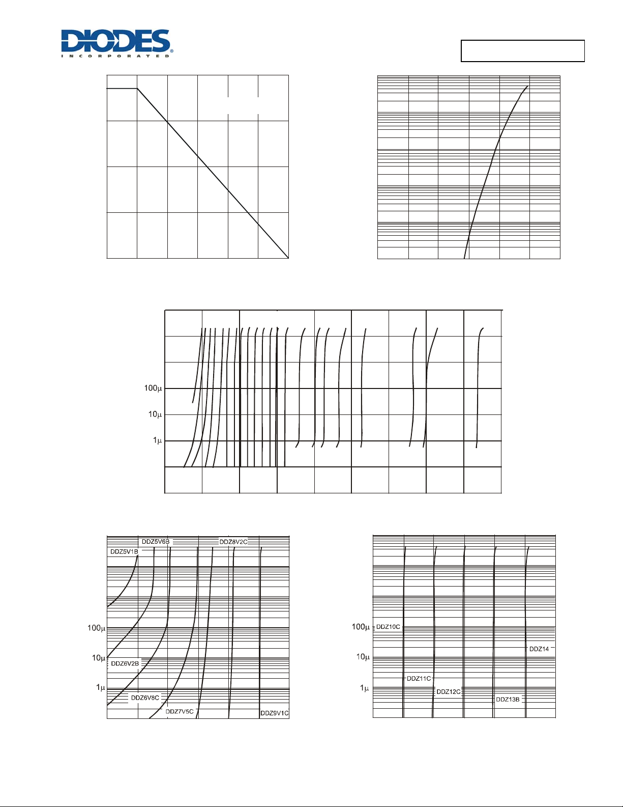
Fig. 1 Power Derating Curve
°
ANE
I, INS
F
0.1
0.01
0
V , INSTANTANEOUS FORWARD VOLTAGE (V)
F
0.2
0.4
0.6 0.8
Fig. 2 Typical Forward Characteristics
1.0
1.2
100m
20C
14
15
11C
13B
5V6B
5V1B
6V2B
10C
12C
8V2C
9V1C
7V5C
6V8C
16
18C
22D
24C
27D
36
33
43
10m
100m
10m
(A)
1m
E
E
1m
(A)
Z
I, ZENE
100n
10n
05
10 15
20
V , ZENER VOLTAGE (V)
Z
25 30 35 40 45
Fig. 3 Typical Zener Brea kdown Ch ar acteristics
100m
10m
(A)
1m
E
Z
I, ZE
100n
4.0 6.0 8.0 10.0
5.0 7.0 9.0
V , ZENER VOLTAGE (V)
Z
Fig. 4 Typical Zener Breakdown Characteristics,
DDZ5V1B - DDZ9V1
DDZ5V1B - DDZ43
Document number: DS30407 Rev. 13 - 2
3 of 7
www.diodes.com
Z
I, ZE
100n
10.0
8.0 11.0 13.0 15.0
V , ZENER VOLTAGE (V)
Z
12.0 14.0
Fig. 5 Typical Zen er B r ea kdown Cha r acteri s t ics,
DDZ10C - DDZ14
December 2013
© Diodes Incorporated
Page 4

N
R
CUR
R
N
T
C
N
R CUR
REN
T
C
R CUR
RENT
R CUR
RENT
C
100m
10m
(A)
1m
100m
10m
(A)
1m
DDZ5V1B - DDZ43
E
E
Z
I, ZE
100n
15 17
14
16
V , ZENER VOLTAGE (V)
Z
Fig. 6 Typical Zener Brea kdown Ch ar acteristics,
DDZ15 - DDZ18
100m
10m
18
19
20
E
Z
I, ZE
100n
19 21 23
20
V , ZENER VOLTAGE (V)
Z
Fig. 7 Typical Zener Breakdown Cha r acteri s t ics,
DDZ20C - DDZ24
100m
10m
22
24
25
(A)
1m
Z
I, ZENE
100n
26 30
28 32 36
V , ZENER VOLTAGE (V)
Z
Fig. 8 Typical Zener Br eakdown Character istics,
DDZ27D - DDZ36
100
V =1V
R
V = 2V
R
10
34
T = 25 °C
J
f = 1MHz
38
(A)
1m
Z
I, ZENE
100n
38
42
40 44
V , ZENER VOLTAGE (V)
Z
46
48
Fig. 9 Typical Zener Br eakdown Character istics, DDZ43
10,000
1,000
100
10
50
T
C , TOT AL CAPACITANCE (pF)
1
1
V , NOMINAL ZENER VOLT AGE (V)
Z
10
Fig. 10 Typical Total Capacitance vs. Nominal Zener Voltage
DDZ5V1B - DDZ43
Document number: DS30407 Rev. 13 - 2
100
4 of 7
www.diodes.com
1
0.1
6.0
5.0
7.0
V , ZENER VOLTAGE (V)
Z
8.0
9.0 10.0
Fig. 11 Typica l Z ener Impedance Chara ct er istics,
DDZ5V6B - DDZ12
11.0
12
December 2013
© Diodes Incorporated
Page 5

C
C
T
C
TEMPER
T
U
RE C
OEF
FICIEN
T
T
C
T
P
R
TURE C
O
F
F
C
T
DDZ5V1B - DDZ43
10,000
1,000
100
10
0.1
10,000
1,000
1
12
13 14
V , ZENER VOLT AGE (V)
Z
15
16
17
Fig. 12 Typical Zener Impedance Characteristics,
DDZ12C - DDZ18
18
10,000
1,000
100
10
1
0.1
18 19 20
Fig. 13 Typical Zener Imp edance Cha racteristics,
10,000
1,000
21
22 23
V , ZENER VOLTAGE (V)
Z
DDZ18C - DDZ24
24
100
10
1
0.1
24
26
28
V , ZENER VOLT AGE (V)
Z
30
32 34
Fig. 14 Typical Zener Impedance Characteristics,
DDZ24C - DDZ33
0.12
0.10
0.08
0.06
0.04
0.02
A
0
-0.02
Z
OF ZENER VOLTAGE (%/°C)
-0.04
of V ,
-0.06
-0.08
0610
42
V , ZENER VOLTAGE (V)
Z
8
Fig. 16 Typical Temperature Coefficient of
Zener Volt age vs. Zener Voltage, DDZ5V1B-DDZ 10C
DDZ5V1B - DDZ43
Document number: DS30407 Rev. 13 - 2
5 of 7
www.diodes.com
IEN
I
E
A
E
EM
Z
of V ,
100
10
1
0.1
36
38 40
V , ZENER VOLTAGE (V)
Z
42
44
Fig. 15 Typical Zener Impedance Characteristics,
DDZ36 - DDZ43
0.12
0.10
0.08
0.06
0.04
0.02
0
-0.02
OF ZENER VOLT AGE (%/°C)
-0.04
-0.06
-0.08
10
12
14
V , ZENER VOLTAGE (V )
Z
16 20
Fig. 17 Typical Temperature Coefficient of
Zener Voltage vs. Zener Voltage, DDZ10C-DDZ20C
46
48
18
December 2013
© Diodes Incorporated
Page 6

T
C
TEMPERATUR
C
O
F
FICIEN
T
T
C
T
P
RATURE C
O
F
FICIEN
T
0.12
0.10
0.08
0.06
E
0.04
E
0.02
0
-0.02
Z
OF ZENER VOLTAGE (%/°C)
-0.04
of V ,
-0.06
-0.08
20
22
Fig. 18 Typical T emperature Coefficient of
Zener Volt age vs. Zener Voltage, DDZ20 C - DD Z 30D
24
V , ZENER VOLTAGE (V)
Z
26 30
28
E
E
EM
Z
of V ,
0.12
0.10
0.08
0.06
0.04
0.02
0
-0.02
OF ZENER VOLT AGE (%/°C)
-0.04
-0.06
-0.08
30
34
V , ZENER VOLTAGE (V)
Fig. 19 Typical Temper at ur e Coeffici ent of
Zener Voltage vs. Zener Voltage, DDZ30 D - DDZ43
Z
DDZ5V1B - DDZ43
38
42 50
46
Package Outline Dimensions
Please see AP02002 at http://www.diodes.com/datasheets/ap02002.pdf for latest version.
B
M
C
H
SOD123
Dim Min Max
A
A 0.55 Typ
B 1.40 1.70
C 3.55 3.85
H 2.55 2.85
J 0.00 0.10
K 1.00 1.35
K
L
L 0.25 0.40
M 0.10 0.15
α
0 8°
All Dimensions in mm
Suggested Pad Layout
Please see AP02001 at http://www.diodes.com/datasheets/ap02001.pdf for the latest version.
Y
DDZ5V1B - DDZ43
Document number: DS30407 Rev. 13 - 2
X1
X
Dimensions Value (in mm)
G 2.250
X 0.900
X1 4.050
Y 0.950
G
6 of 7
www.diodes.com
December 2013
© Diodes Incorporated
Page 7

IMPORTANT NOTICE
DIODES INCORPORATED MAKES NO WARRANTY OF ANY KIND, EXPRESS OR IMPLIED, WITH REGARDS TO THIS DOCUMENT,
INCLUDING, BUT NOT LIMITED TO, THE IMPLIED WARRANTIES OF MERCHANTABILITY AND FITNESS FOR A PARTICULAR PURPOSE
(AND THEIR EQUIVALENTS UNDER THE LAWS OF ANY JURISDICTION).
Diodes Incorporated and its subsidiaries reserve the right to make modifications, enhancements, improvements, corrections or other changes
without further notice to this document and any product described herein. Diodes Incorporated does not assume any liability arising out of the
application or use of this document or any product described herein; neither does Diodes Incorporated convey any license under its patent or
trademark rights, nor the rights of others. Any Customer or user of this document or products described herein in such applications shall assume
all risks of such use and will agree to hold Diodes Incorporated and all the companies whose products are represented on Diodes Incorporated
website, harmless against all damages.
Diodes Incorporated does not warrant or accept any liability whatsoever in respect of any products purchased through unauthorized sales channel.
Should Customers purchase or use Diodes Incorporated products for any unintended or unauthorize d application, Customers shall indemnify and
hold Diodes Incorporated and its representatives harmless against all claims, damages, expenses, and attorney fees arising out of, directly or
indirectly, any claim of personal injury or death associated with such unintended or unauthorized application.
Products described herein may be covered by one or more United States, international or foreign patents pending. Product names and markings
noted herein may also be covered by one or more United States, international or foreign trademarks.
This document is written in English but may be translated into multiple languages for reference. Onl y the English version of this document is the
final and determinative format released by Diodes Incorporated.
LIFE SUPPORT
Diodes Incorporated products are specifically not authorized for use as critical components in life support devices or systems without the express
written approval of the Chief Executive Officer of Diodes Incorporated. As used herein:
A. Life support devices or systems are devices or systems which:
1. are intended to implant into the body, or
2. support or sustain life and whose failure to perform when properly used in accordance with instructions for use provided in th e
labeling can be reasonably expected to result in significant injury to the user.
B. A critical component is any component in a life support device or system whose failure to perform can be reasonably expected to cause the
failure of the life support device or to affect its safety or effectiveness.
Customers represent that they have all necessary expertise in the safety and regulatory ramifications of their life support devices or systems, and
acknowledge and agree that they are solely responsible for all legal, regulatory and safety-related requirements concerning their products and any
use of Diodes Incorporated products in such safety-critical, life support devices or systems, notwithstanding any devices- or systems-related
information or support that may be provided by Diodes Incorporated. Further, Customers must fully indemnify Diodes Incorporated and its
representatives against any damages arising out of the use of Diodes Incorporated products in such safety-critical, life support devices or systems.
Copyright © 2013, Diodes Incorporated
www.diodes.com
DDZ5V1B - DDZ43
DDZ5V1B - DDZ43
Document number: DS30407 Rev. 13 - 2
7 of 7
www.diodes.com
December 2013
© Diodes Incorporated
 Loading...