

Page 1
Features
• 500mW Power Dissipation on FR-4 PCB
• Very Tight Tolerance on V
• Ideally Suited for Automated Assembly Processes
• Lead, Halogen and Antimony Free, RoHS Compliant (Note 1)
• Halogen and Antimony Free "Green" Device (Notes 2 & 3)
•
NEW PRODUCT
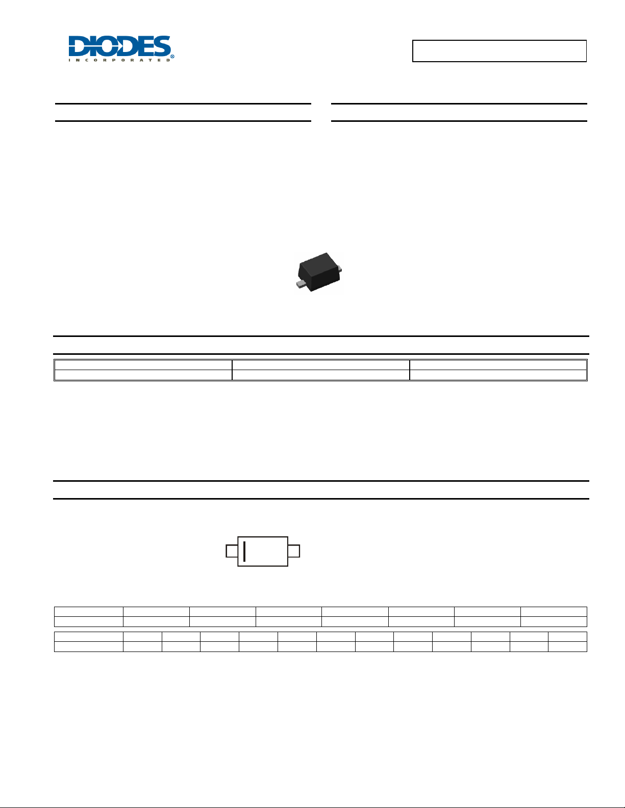
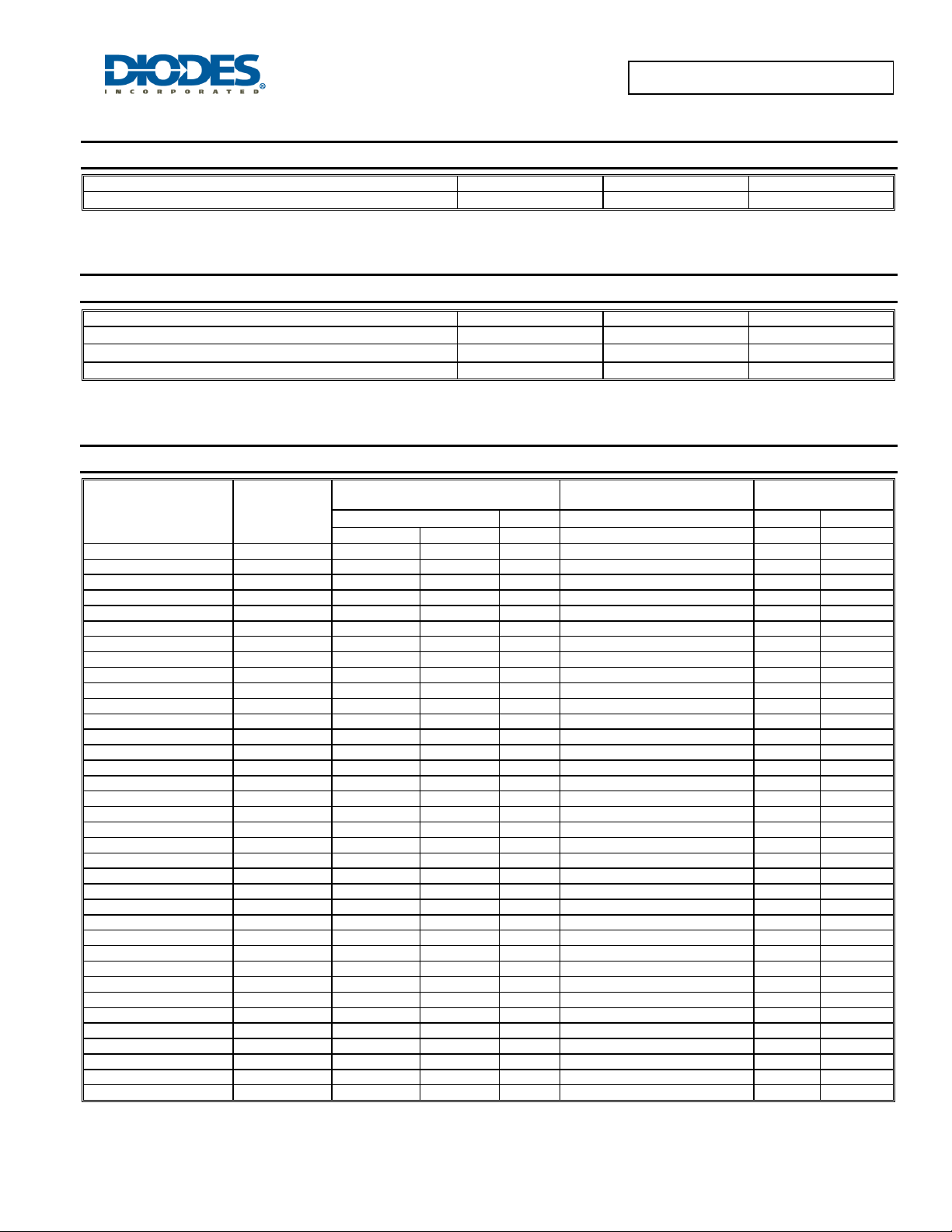
Z
Top View
DDZ2V4ASF –DDZ39DSF
0.5W SURFACE MOUNT PRECISION ZENER DIODE
Mechanical Data
• Case: SOD323F
• Case Material: Molded Plastic, “Green Molding Compound”.
UL Flammability Classification Rating 94V-0
• Moisture Sensitivity: Level 1 per J-STD-020
• Terminal Connections: Cathode Band
• Terminals: Finish - Matte Tin annealed over Copper Alloy
leadframe. Solderable per MIL-STD-202, Method 208
• Weight: 0.01 grams (approximate)
Ordering Information (Note 4)
Part Number Case Packaging
DDZxx(x)xSF-7* SOD323F 3000/Tape & Reel
* Add "-7" to the appropriate type number in Electrical Characteristics Table on page 2. Example: DDZ10BSF-7.
Notes: 1. Fully EU Directive 2002/95/EC (RoHS) & 2011/65/EU (RoHS 2) compliant. No purposely added lead.
<1000ppm antimony compounds.
2. Halogen and Antimony free "Green” products are defined as those which contain <900ppm bromine, <900ppm chlorine (<1500ppm total Br + Cl) and
3. Diodes Inc.'s "Green" policy can be found on our website at http://www.diodes.com.
4. For packaging details, go to our website at http://www.diodes.com.
Marking Information
Date Code Key
Year 2010 2011 2012 2013 2014 2015 2016
Code X Y Z A B C D
Month Jan Feb Mar Apr May Jun Jul Aug Sep Oct Nov Dec
Code 1 2 3 4 5 6 7 8 9 O N D
XX
YM
xx = Product Type Marking Code
(See Electrical Characteristics Table)
YM = Date Code Marking
Y = Year (ex: W = 2009)
M = Month (ex: 9 = September)
DDZ2V4ASF – DDZ39DSF
Document number: DS31987 Rev. 17 - 2
1 of 6
www.diodes.com
March 2012
© Diodes Incorporated
Page 2
θ
μ
Maximum Ratings @T
Forward Voltage @ IF = 10mA VF
= 25°C unless otherwise specified
A
Characteristic Symbol Value Unit
DDZ2V4ASF –DDZ39DSF
0.9 V
Thermal Characteristics
Characteristic Symbol Value Unit
Power Dissipation (Note 5)
Thermal Resistance, Junction to Ambient Air (Note 5)
Operating and Storage Temperature Range
Electrical Characteristics @T
NEW PRODUCT
Type Number Marking Code
DDZ2V4ASF 4C 2.33 2.52 20 100 120 1
DDZ2V4BSF KD 2.43 2.63 20 100 120 1
DDZ2V7ASF 4E 2.54 2.75 20 110 120 1
DDZ2V7BSF KE 2.69 2.91 20 110 120 1
DDZ3V0ASF 4F 2.85 3.07 20 120 50 1
DDZ3V0BSF KF 3.01 3.22 20 120 50 1
DDZ3V3ASF 4G 3.16 3.38 20 130 20 1
DDZ3V3BSF KG 3.32 3.53 20 130 20 1
DDZ3V6ASF 4H 3.45 3.69 20 130 10 1
DDZ3V6BSF KH 3.60 3.84 20 130 10 1
DDZ3V9ASF 4J 3.74 4.01 20 130 10 1
DDZ3V9BSF KJ 3.89 4.16 20 130 10 1
DDZ4V3ASF 4K 4.04 4.29 20 130 10 1
DDZ4V3BSF KK 4.17 4.43 20 130 10 1
DDZ4V3CSF YK 4.30 4.57 20 130 10 1
DDZ4V7ASF 4L 4.44 4.68 20 130 10 1
DDZ4V7BSF KL 4.55 4.80 20 130 10 1
DDZ4V7CSF YL 4.68 4.93 20 130 10 1
DDZ5V1ASF 4M 4.81 5.07 20 130 7.5 2
DDZ5V1BSF KM 4.94 5.20 20 130 7.5 2
DDZ5V1CSF YM 5.09 5.37 20 130 7.5 2
DDZ5V6ASF 4N 5.28 5.55 20 80 7.5 2
DDZ5V6BSF KN 5.45 5.73 20 80 7.5 2
DDZ5V6CSF YN 5.61 5.91 20 80 7.5 2
DDZ6V2ASF 4O 5.78 6.09 20 50 7.5 3
DDZ6V2BSF KO 5.96 6.27 20 50 7.5 3
DDZ6V2CSF YO 6.12 6.44 20 50 7.5 3
DDZ6V8ASF 4P 6.29 6.63 20 30 7.5 4
DDZ6V8BSF KP 6.49 6.83 20 30 7.5 4
DDZ6V8CSF YP 6.66 7.01 20 30 7.5 4
DDZ7V5ASF 4Q 6.85 7.22 20 30 7.5 4
DDZ7V5BSF KQ 7.07 7.45 20 30 7.5 4
DDZ7V5CSF YQ 7.29 7.67 20 30 7.5 4
DDZ8V2ASF 4R 7.53 7.92 20 30 7.5 7.15
DDZ8V2BSF KR 7.78 8.19 20 30 7.5 7.39
DDZ8V2CSF YR 8.03 8.45 20 30 7.5 7.63
Notes: 5. Device mounted on FR-4 PCB with 10mm x 10mm pad, board size 35mm * 25mm.
6. The Zener voltage is measured 40ms after power is supplied.
7. Short duration pulse test used to minimize self-heating effect.
DDZ2V4ASF – DDZ39DSF
Document number: DS31987 Rev. 17 - 2
= 25°C unless otherwise specified
A
Zener Voltage Range
(Notes 6 & 7)
VZ @ IZT IZT Z
Min (V) Max (V) mA
www.diodes.com
2 of 6
P
R
T
J, TSTG
D
JA
Maximum Zener Impedance
500 mW
250
-65 to +150
f = 1kHz
ZT @ IZT
Ω
I
°C/W
°C
Maximum Reverse
Current (Note 8)
@ VR
R
A
© Diodes Incorporated
V
March 2012
Page 3

μ
Electrical Characteristics (continued) @T
Zener Voltage Range
Type Number Marking Code
DDZ9V1ASF 4S 8.29 8.73 20 30 7.5 7.88
DDZ9V1BSF KS 8.57 9.01 20 30 7.5 8.14
DDZ9V1CSF YS 8.83 9.30 20 30 7.5 8.39
DDZ10ASF 4T 9.12 9.59 20 30 7.5 8.66
DDZ10BSF KT 9.41 9.90 20 30 7.5 8.94
DDZ10CSF YT 9.70 10.20 20 30 7.5 9.22
DDZ10DSF 7T 9.94 10.44 20 30 7.5 9.44
DDZ11ASF 4U 10.18 10.71 10 30 0.07 9.67
DDZ11BSF KU 10.50 11.05 10 30 7.5 9.98
DDZ11CSF YU 10.82 11.38 10 30 0.07 10.28
DDZ12ASF 4V 11.13 11.71 10 35 0.07 10.60
DDZ12BSF KV 11.44 12.03 10 30 0.07 10.90
DDZ12CSF YV 11.74 12.35 10 35 0.07 11.20
DDZ13ASF 4W 12.11 12.75 10 35 0.07 11.50
DDZ13BSF KW 12.55 13.21 10 35 0.07 11.90
DDZ13CSF YW 12.99 13.66 10 35 0.07 12.30
NEW PRODUCT
DDZ15ASF 4X 13.44 14.13 10 40 0.07 12.80
DDZ15BSF KX 13.89 14.62 10 40 0.07 13.20
DDZ15CSF YX 14.35 15.09 10 40 0.07 13.60
DDZ16ASF 4Y 14.80 15.57 10 40 0.07 14.10
DDZ16BSF KY 15.25 16.04 10 40 0.07 14.50
DDZ16CSF YY 15.69 16.51 10 40 0.07 14.90
DDZ18ASF 4Z 16.22 17.06 10 45 0.07 15.40
DDZ18BSF KZ 16.82 17.70 10 45 0.07 16.00
DDZ18CSF YZ 17.42 18.33 10 45 0.07 16.50
DDZ20ASF RJ 18.05 18.96 10 50 0.07 17.10
DDZ20BSF ZJ 18.63 19.59 10 50 0.07 17.70
DDZ20CSF PJ 19.23 20.22 10 50 0.07 17.70
DDZ20DSF 2J 19.72 20.72 10 50 0.07 18.70
DDZ22ASF RK 20.15 21.20 5 55 0.07 19.10
DDZ22BSF ZK 20.64 21.71 5 55 0.07 19.60
DDZ22CSF PK 21.08 22.17 5 55 0.07 20.00
DDZ22DSF 2K 21.52 22.63 5 55 0.07 20.40
DDZ24ASF RL 22.05 23.18 5 60 0.07 20.90
DDZ24BSF ZL 22.61 23.77 5 60 0.07 21.50
DDZ24CSF PL 23.12 24.31 5 60 0.07 22.00
DDZ24DSF 2L 23.63 24.85 5 60 0.07 22.40
DDZ27ASF RM 24.26 25.52 5 70 0.07 23.00
DDZ27BSF ZM 24.97 26.26 5 70 0.07 23.70
DDZ27CSF PM 25.63 26.95 5 70 0.07 24.30
DDZ27DSF 2M 26.29 27.64 5 70 0.07 25.00
DDZ30ASF RN 26.99 28.39 5 80 0.07 25.60
DDZ30BSF ZN 27.70 29.13 5 80 0.07 26.00
DDZ30CSF PN 28.36 29.82 5 55 0.07 26.90
DDZ30DSF 2N 29.02 30.51 5 80 0.07 27.60
DDZ33ASF RO 29.68 31.22 5 80 0.07 28.20
DDZ33BSF ZO 30.32 31.88 5 80 0.07 28.80
DDZ33CSF PO 30.90 32.50 5 65 0.07 29.40
DDZ33DSF 2O 31.49 33.11 5 65 0.07 29.90
DDZ36ASF RP 32.14 33.79 5 90 0.07 30.50
DDZ36BSF ZP 32.79 34.49 5 90 0.07 31.20
DDZ36CSF PP 33.40 35.13 5 75 0.07 31.70
DDZ36DSF 2P 34.01 35.77 5 90 0.07 32.30
DDZ39ASF RQ 34.68 36.47 5 85 0.2 30.00
DDZ39BSF ZQ 35.36 37.19 5 85 0.2 30.00
DDZ39CSF PQ 36.00 37.85 5 85 0.2 30.00
DDZ39DSF 2Q 36.63 38.52 5 85 0.2 30.00
Notes: 5. Device mounted on FR-4 PCB with 10mm x 10mm pad, board size 35mm * 25mm.
6. The Zener voltage is measured 40ms after power is supplied.
7. Short duration pulse test used to minimize self-heating effect.
DDZ2V4ASF – DDZ39DSF
Document number: DS31987 Rev. 17 - 2
VZ @ IZT IZT Z
Min (V) Max (V) mA
= 25°C unless otherwise specified
A
(Note 6)
3 of 6
www.diodes.com
Maximum Zener Impedance
DDZ2V4ASF –DDZ39DSF
f = 1kHz
ZT @ IZT
Ω
I
Maximum Reverse
Current (Note 7)
@ VR
R
A
March 2012
© Diodes Incorporated
V
Page 4

P, P
OWER
P
T
O
TANT
O
U
O
RWARD CUR
RENT
T
C
TEMPERATURE C
O
CIEN
T
C
R C
U
R
R
T
NEW PRODUCT
DDZ2V4ASF –DDZ39DSF
0.6
1
(A)
R = 250°C/W
θ
0.5
JA
N (W)
I
0.4
Note 5
0.1
A
0.3
DISSI
0.2
D
0.1
0
50
)
250 50 75 100 125 150
T , AMBIENT TEMPERATURE ( C)
A
Fig. 1 Power Derating Curve
°
S F
ANE
F
I , INS
0.001
T = 150°C
0.01
0.2
V , INSTANTANEOUS FORW ARD VOLTAGE (V)
F
T = 125°C
A
T = 105°C
A
T = 85°C
A
0.4
A
0.6 0.8
Fig. 2 Typical Forward Characteristics
T = 25°C
A
T = -40°C
A
T = -65°C
A
1.0
1.2
40
30
(mV/°
20
10
EFFI
0
-10
-20
-30
,
-40
-50
010203040
V , ZENER VOLTAGE (V)
Z
Fig. 3 Temperature Coefficient vs. Zener Voltage
20
16
(mA)
EN
12
8
3V6BSF
5V1BSF
5V6BSF
6V2BSF
10BSF
11BSF
12BSF
15BSF
18BSF
20BSF
24BSF
27DSF
30BSF
36BSF
Z
I, ZENE
4
0
0 2 4 6 8 10121416182022
V , ZENE R VOLTAGE (V)
Fig. 4 Typical Characteristics
Z
Zener Breakdown
24 26 28 36
30 32 34
DDZ2V4ASF – DDZ39DSF
Document number: DS31987 Rev. 17 - 2
4 of 6
www.diodes.com
March 2012
© Diodes Incorporated
Page 5

α
Package Outline Dimensions
NEW PRODUCT
He
E
A
D
b (2x)
DDZ2V4ASF –DDZ39DSF
c
α
1
β
1
β
2
2
L1
L2 (2x)
b (2x)
Dim Min Max Typ
SOD323F
A 0.60 0.75
b 0.25 0.35
c 0.05 0.26
D 1.15 1.35 1.25
E 1.60 1.80 1.70
He 2.30 2.70 2.50
L1 0.30 0.50 0.40
L2 0.41 0.61 0.51
α1
α2
β1
β2
− −
− −
− −
− −
All Dimensions in mm
−
−
−
7°
3°
7°
3°
Suggested Pad Layout
DDZ2V4ASF – DDZ39DSF
Document number: DS31987 Rev. 17 - 2
X1
Y (2x)
X (2x)
5 of 6
www.diodes.com
Dimensions Value (in mm)
X 0.710
X1 2.700
Y 0.403
March 2012
© Diodes Incorporated
Page 6

DIODES INCORPORATED MAKES NO WARRANTY OF ANY KIND, EXPRESS OR IMPLIED, WITH REGARDS TO THIS DOCUMENT,
INCLUDING, BUT NOT LIMITED TO, THE IMPLIED WARRANTIES OF MERCHANTABILITY AND FITNESS FOR A PARTICULAR PURPOSE
(AND THEIR EQUIVALENTS UNDER THE LAWS OF ANY JURISDICTION).
Diodes Incorporated and its subsidiaries reserve the right to make modifications, enhancements, improvements, corrections or other changes
without further notice to this document and any product described herein. Diodes Incorporated does not assume any liability arising out of the
application or use of this document or any product described herein; neither does Diodes Incorporated convey any license under its patent or
trademark rights, nor the rights of others. Any Customer or user of this document or products described herein in such applications shall assume
all risks of such use and will agree to hold Diodes Incorporated and all the companies whose products are represented on Diodes Incorporated
website, harmless against all damages.
Diodes Incorporated does not warrant or accept any liability whatsoever in respect of any products purchased through unauthorized sales channel.
Should Customers purchase or use Diodes Incorporated products for any unintended or unauthorize d application, Customers shall indemnify and
hold Diodes Incorporated and its representatives harmless against all claims, damages, expenses, and attorney fees arising out of, directly or
indirectly, any claim of personal injury or death associated with such unintended or unauthorized application.
NEW PRODUCT
Products described herein may be covered by one or more United States, international or foreign patents pending. Product names and markings
noted herein may also be covered by one or more United States, international or foreign trademarks.
Diodes Incorporated products are specifically not authorized for use as critical components in life support devices or systems without the express
written approval of the Chief Executive Officer of Diodes Incorporated. As used herein:
A. Life support devices or systems are devices or systems which:
1. are intended to implant into the body, or
labeling can be reasonably expected to result in significant injury to the user.
B. A critical component is any component in a life support device or system whose failure to perform can be reasonably expected to cause the
failure of the life support device or to affect its safety or effectiveness.
Customers represent that they have all necessary expertise in the safety and regulatory ramifications of their life support devices or systems, and
acknowledge and agree that they are solely responsible for all legal, regulatory and safety-related requirements concerning their products and any
use of Diodes Incorporated products in such safety-critical, life support devices or systems, notwithstanding any devices- or systems-related
information or support that may be provided by Diodes Incorporated. Further, Customers must fully indemnify Diodes Incorporated and its
representatives against any damages arising out of the use of Diodes Incorporated products in such safety-critical, life support devices or systems.
Copyright © 2012, Diodes Incorporated
www.diodes.com
2. support or sustain life and whose failure to perform when properly used in accordance with instructions for use provided in the
IMPORTANT NOTICE
LIFE SUPPORT
DDZ2V4ASF –DDZ39DSF
DDZ2V4ASF – DDZ39DSF
Document number: DS31987 Rev. 17 - 2
6 of 6
www.diodes.com
March 2012
© Diodes Incorporated
 Loading...