

Page 1
PNP PRE-BIASED SMALL SIGNAL SURFACE MOUNT TRANSISTOR
Features
• Epitaxial Planar Die Construction
• Complementary NPN Types Available (DDTC)
• Built-In Biasing Resistors, R1≠R2
• “Lead Free”, RoHS Compliant (Note 1)
• Halogen and Antimony Free "Green" Device (Note 2)
• Qualified to AEC-Q101 Standards for High Reliability
Part Number R1 (NOM) R2 (NOM) Marking
DDTA113ZE
DDTA123YE
DDTA123JE
DDTA143XE
DDTA143FE
DDTA143ZE
DDTA114YE
DDTA114WE
DDTA124XE
DDTA144VE
DDTA144WE
1KΩ 10KΩ
2.2KΩ 10KΩ
2.2KΩ 47KΩ
4.7KΩ 10KΩ
4.7KΩ 22KΩ
4.7KΩ 47KΩ
10KΩ 47KΩ
10KΩ 4.7KΩ
22KΩ 47KΩ
47KΩ 10KΩ
47KΩ 22KΩ
SOT523
Top View
Mechanical Data
• Case: SOT523
• Case Material: Molded Plastic, “Green” Molding Compound,
Note 3. UL Flammability Classification Rating 94V-0
• Moisture Sensitivity: Level 1 per J-STD-020
• Terminals: Matte Tin Finish annealed over Alloy 42 leadframe
(Lead Free Plating) Solderable per MIL-STD-202, Method 208
• Weight: 0.002 grams (approximate)
P02
P05
P06
P09
P10
P11
P14
P15
P18
P21
P22
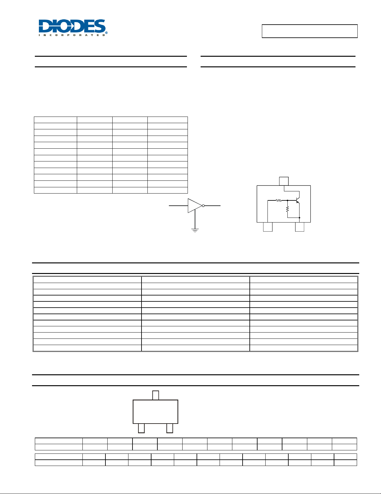
IN OUT
1 3
2
E
GND (+)
CB
Device Schematic
DDTA (R1≠R2 SERIES)
OUT
3
C
R1
B
R2
E
21
IN
Package Pin Out
Configuration
GND(+)
Ordering Information (Note 3)
Part Number Case Packaging
DDTA113ZE-7-F SOT523 3000/Tape & Reel
DDTA123YE-7-F SOT523 3000/Tape & Reel
DDTA123JE-7-F SOT523 3000/Tape & Reel
DDTA143XE-7-F SOT523 3000/Tape & Reel
DDTA143FE-7-F SOT523 3000/Tape & Reel
DDTA143ZE-7-F SOT523 3000/Tape & Reel
DDTA114YE-7-F SOT523 3000/Tape & Reel
DDTA114WE-7-F SOT523 3000/Tape & Reel
DDTA124XE-7-F SOT523 3000/Tape & Reel
DDTA144VE-7-F SOT523 3000/Tape & Reel
DDTA144WE-7-F SOT523 3000/Tape & Reel
Notes: 1. No purposefully added lead.
2. Diodes Inc.'s "Green" policy can be found on our website at http://www.diodes.com.
3. For packaging details, go to our website at http://www.diodes.com.
Marking Information
Date Code Key
Year 2005 2006 2007 2008 2009 2010 2011 2012 2013 2014 2015
Code S T U V W X Y Z A B C
Month Jan Feb Mar Apr May Jun Jul Aug Sep Oct Nov Dec
Code 1 2 3 4 5 6 7 8 9 O N D
Pxx
YM
Pxx = Product Type Marking Code (See Features Table)
YM = Date Code Marking
Y = Year (ex: T = 2006)
M = Month (ex: 9 = September)
DDTA (R1≠R2 SERIES) E
Document number: DS30318 Rev. 8 - 2
1 of 6
www.diodes.com
November 2011
© Diodes Incorporated
Page 2
)
θ
Maximum Ratings @T
= 25°C unless otherwise specified
A
Characteristic Symbol Value Unit
Supply Voltage, (2) to (3)
DDTA113ZE
DDTA123YE
DDTA123JE
DDTA143XE
DDTA143FE
Input Voltage, (1) to (2)
DDTA143ZE
DDTA114YE
DDTA114WE
DDTA124XE
DDTA144VE
DDTA144WE
DDTA113ZE
DDTA123YE
DDTA123JE
DDTA143XE
DDTA143FE
Output Current
DDTA143ZE
DDTA114YE
DDTA114WE
DDTA124XE
DDTA144VE
DDTA144WE
Output Current All
VCC
VIN
IO
I
C(MAX
DDTA (R1≠R2 SERIES)
-50 V
+5 to -10
+5 to -12
+5 to -12
+7 to -20
+6 to -30
+5 to -30
+6 to -40
+10 to -30
+10 to -40
+15 to -40
+10 to -40
-100
-100
-100
-100
-100
-100
-70
-100
-50
-30
-30
-100 mA
V
mA
Thermal Characteristics
Power Dissipation
Thermal Resistance, Junction to Ambient Air (Note 4)
Operating and Storage Temperature Range
DDTA (R1≠R2 SERIES) E
Document number: DS30318 Rev. 8 - 2
Characteristic Symbol Value Unit
P
D
R
JA
T
, T
J
2 of 6
www.diodes.com
STG
150 mW
833
-55 to +150
°C/W
°C
November 2011
© Diodes Incorporated
Page 3

)
DDTA (R1≠R2 SERIES)
Electrical Characteristics @T
= 25°C unless otherwise specified
A
Characteristic Symbol Min Typ Max Unit Test Condition
DDTA113ZE
DDTA123YE
DDTA123JE
DDTA143XE
DDTA143FE
DDTA143ZE
DDTA114YE
V
l(OFF)
DDTA114WE
DDTA124XE
DDTA144VE
DDTA144WE
Input Voltage
DDTA113ZE
DDTA123YE
DDTA123JE
DDTA143XE
DDTA143FE
DDTA143ZE
DDTA114YE
V
l(ON)
DDTA114WE
DDTA124XE
DDTA144VE
DDTA144WE
Output Voltage
V
O(ON)
DDTA113ZE
DDTA123YE
DDTA123JE
DDTA143XE
DDTA143FE
Input Current
DDTA143ZE
I
DDTA114YE
DDTA114WE
DDTA124XE
DDTA144VE
DDTA144WE
Output Current
I
O(OFF
DDTA113ZE
DDTA123YE
DDTA123JE
DDTA143XE
DDTA143FE
DC Current Gain
DDTA143ZE
DDTA114YE
DDTA114WE
DDTA124XE
G
DDTA144VE
DDTA144WE
Input Resistor Tolerance
Resistance Ratio Tolerance
Gain-Bandwidth Product*
* Transistor – F or Reference Only
Notes: 4. Mounted on FR4 PC Board with recommended pad layout at http://www .diodes.com.
ΔR
ΔR
2/R1
f
T
-0.3
-0.3
-0.5
-0.3
-0.3
-0.5
⎯ ⎯
-0.3
V
V
= -5V, IO = -100μA
CC
-0.8
-0.4
-1.0
-0.8
V
= -0.3V, IO = -20mA
O
= -0.3V, IO = -20mA
V
O
V
= -0.3V, IO = -5mA
O
= -0.3V, IO = -20mA
V
O
V
= -0.3V, IO = -3mA
O
= -0.3V, IO = -5mA
V
O
V
= -0.3V, IO = -1mA
O
= -0.3V, IO = -2mA
V
O
V
= -0.3V, IO = -2mA
O
= -0.3V, IO = -2mA
V
O
V
= -0.3V, IO = -2mA
O
I
= -5mA/-0.25mA DDTA123E
O/Il
= -5mA/-0.25mA DDTA143E
I
O/Il
I
= -5mA/-0.25mA DDTA114E
O/Il
= -10mA/-0.5mA All Others
I
O/Il
-3.0
-3.0
-1.1
-2.5
-1.3
⎯ ⎯
-1.3
-1.4
-3.0
-2.5
-5.0
-4.0
-0.1 -0.3 V
⎯
-7.2
-3.8
-3.6
-1.8
-1.8
l
⎯ ⎯
-1.8
-0.88
mA
V
= -5V
I
-0.88
-0.36
-0.16
-0.16
⎯ ⎯
-0.5
μA
VCC = -50V, VI = 0V
33
33
80
30
68
80
68
24
l
68
⎯
⎯
VO = -5V, IO = -10mA
⎯
33
56
-30
1
-20
⎯
+30 %
⎯
+20 %
⎯
250
⎯
MHz
⎯
⎯
VCE = -10V, IE = 5mA, f = 100MHz
DDTA (R1≠R2 SERIES) E
Document number: DS30318 Rev. 8 - 2
3 of 6
www.diodes.com
November 2011
© Diodes Incorporated
Page 4

P, P
O
R
P
TIO
C CUR
R
T
G
C
O
CTO
R
T
TER
CAPACITAN
C
F
C
O
C
T
O
R
C
U
R
RENT
DDTA (R1≠R2 SERIES)
Typical Curves – DDTA123JE
250
200
N (mW)
150
A
DISSI
100
WE
D
50
0
-50
050100
T , AMBIENT TEMPERATURE ( C)
A
Fig. 1 Power Dissipation vs. Ambient Temperature
1
150
°
1,000
V = 10V
CE
AIN
EN
100
FE
h, D
10
110100
I , COLLECTOR CURRENT (mA)
C
Fig. 2 Typical DC Current Gain vs. Collector Current
12
f = 1MHz
EMI
LLE
0.01
SATURATION VOLT AGE (V)
CE(SAT)
V,
0.001
100
10
(mA)
0.1
0
10 20 30
I , COLLECTOR CURRENT (mA)
C
Fig. 3 Collector Emitter Saturation Voltage
vs. Collector Current
1
40
V = 5V
O
50
10
)
8
E (p
6
4
2
0
0
10
5
V , REVERSE VOLTAGE (V)
R
15
20
Fig. 4 Typical Capacitance Ch ar acteristics
25
30
10
V = 0.2V
O
-25°C
75 C
1
°
0.1
LLE
0.01
C
I,
0.001
0
234
1
V , INPUT VOLTAGE (V)
in
5
67
89
10
Fig. 5 Collector Current vs. Input Voltage
DDTA (R1≠R2 SERIES) E
Document number: DS30318 Rev. 8 - 2
4 of 6
www.diodes.com
in
25°C
V , INPUT VOLTAGE (V)
0.1
0 1020304050
I , COLLECTOR CURRENT (mA)
C
Fig. 6 Input Voltage vs. Collector Current
November 2011
© Diodes Incorporated
Page 5

Package Outline Dimensions
K
J
A
B
G
H
D
Suggested Pad Layout
Y
Z
X E
DDTA (R1≠R2 SERIES)
Dim Min Max Typ
C
N
L
M
C
A 0.15 0.30 0.22
B 0.75 0.85 0.80
C 1.45 1.75 1.60
D
G 0.90 1.10 1.00
H 1.50 1.70 1.60
J 0.00 0.10 0.05
K 0.60 0.80 0.75
L 0.10 0.30 0.22
M 0.10 0.20 0.12
N 0.45 0.65 0.50
α
Dimensions Value (in mm)
SOT523
⎯ ⎯
0° 8°
All Dimensions in mm
Z 1.8
X 0.4
Y 0.51
C 1.3
E 0.7
0.50
⎯
DDTA (R1≠R2 SERIES) E
Document number: DS30318 Rev. 8 - 2
5 of 6
www.diodes.com
November 2011
© Diodes Incorporated
Page 6

IMPORTANT NOTICE
DIODES INCORPORATED MAKES NO WARRANTY OF ANY KIND, EXPRESS OR IMPLIED, WITH REGARDS TO THIS DOCUMENT,
INCLUDING, BUT NOT LIMITED TO, THE IMPLIED WARRANTIES OF MERCHANTABILITY AND FITNESS FOR A PARTICULAR PURPOSE
(AND THEIR EQUIVALENTS UNDER THE LAWS OF ANY JURISDICTION).
Diodes Incorporated and its subsidiaries reserve the right to make modifications, enhancements, improvements, corrections or other changes
without further notice to this document and any product described herein. Diodes Incorporated does not assume any liability arising out of the
application or use of this document or any product described herein; neither does Diodes Incorporated convey any license under its patent or
trademark rights, nor the rights of others. Any Customer or user of this document or products described herein in such applications shall assume
all risks of such use and will agree to hold Diodes Incorporated and all the companies whose products are represented on Diodes Incorporated
website, harmless against all damages.
Diodes Incorporated does not warrant or accept any liability whatsoever in respect of any products purchased through unauthorized sales channel.
Should Customers purchase or use Diodes Incorporated products for any unintended or unauthorize d application, Customers shall indemnify and
hold Diodes Incorporated and its representatives harmless against all claims, damages, expenses, and attorney fees arising out of, directly or
indirectly, any claim of personal injury or death associated with such unintended or unauthorized application.
Products described herein may be covered by one or more United States, international or foreign patents pending. Product names and markings
noted herein may also be covered by one or more United States, international or foreign trademarks.
LIFE SUPPORT
Diodes Incorporated products are specifically not authorized for use as critical components in life support devices or systems without the express
written approval of the Chief Executive Officer of Diodes Incorporated. As used herein:
A. Life support devices or systems are devices or systems which:
1. are intended to implant into the body, or
2. support or sustain life and whose failure to perform when properly used in accordance with instructions for use provided in the
labeling can be reasonably expected to result in significant injury to the user.
B. A critical component is any component in a life support device or system whose failure to perform can be reasonably expected to cause the
failure of the life support device or to affect its safety or effectiveness.
Customers represent that they have all necessary expertise in the safety and regulatory ramifications of their life support devices or systems, and
acknowledge and agree that they are solely responsible for all legal, regulatory and safety-related requirements concerning their products and any
use of Diodes Incorporated products in such safety-critical, life support devices or systems, notwithstanding any devices- or systems-related
information or support that may be provided by Diodes Incorporated. Further, Customers must fully indemnify Diodes Incorporated and its
representatives against any damages arising out of the use of Diodes Incorporated products in such safety-critical, life support devices or systems.
Copyright © 2011, Diodes Incorporated
www.diodes.com
DDTA (R1≠R2 SERIES)
DDTA (R1≠R2 SERIES) E
Document number: DS30318 Rev. 8 - 2
6 of 6
www.diodes.com
November 2011
© Diodes Incorporated
 Loading...