

Page 1
NPN PRE-BIASED SMALL SIGNAL DUAL SURFACE MOUNT TRANSISTOR
Features
• Epitaxial Planar Die Construction
• Complementary PNP Types Available
(DDA)
• Built-In Biasing Resistors
• Lead Free By Design/RoHS Compliant (Note 3)
• "Green" Device (Note 4 and 5)
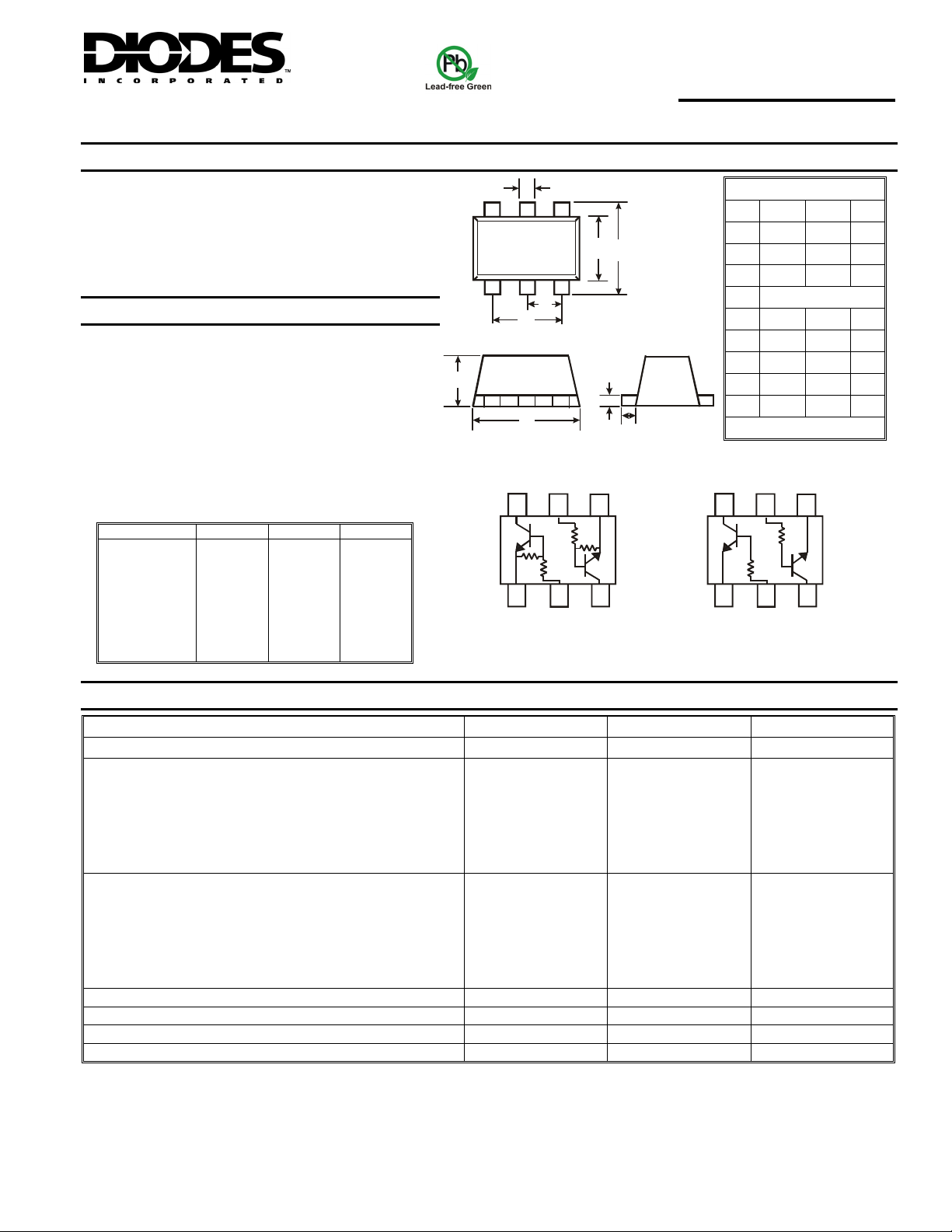
Mechanical Data
• Case: SOT-563
• Case Material: Molded Plastic. UL Flammability
Classification Rating 94V-0
• Moisture Sensitivity: Level 1 per J-STD-020C
• Terminals: Finish - Matte Tin annealed over Alloy 42
leadframe. Solderable per MIL-STD-202, Method 208
• Terminal Connections: See Diagram
• Weight: 0.005 grams (approximate)
P/N R1 R2 MARKING
DDC124EH
DDC144EH
DDC143EH
DDC114YH
DDC123JH
DDC114EH
DDC143TH
DDC114TH
22KΩ
47KΩ
4.7KΩ
10KΩ
2.2KΩ
10KΩ
4.7KΩ
10KΩ
22KΩ
47KΩ
4.7KΩ
47KΩ
47KΩ
10KΩ
⎯
⎯
N17
N20
N08
N14
N06
N13
N07
N12
K
A
NXXYM
D
G
H
SEE NOTE 1
654
R
1
R
R
2
1
21
R1, R2
SCHEMATIC DIAGRAM, TOP VIEW
DDC (xxxx) H
SOT-563
Dim Min Max Typ
A 0.15 0.30 0.25
B
C
M
L
R
2
3
B 1.10 1.25 1.20
C 1.55 1.70 1.60
D 0.50
G 0.90 1.10 1.00
H 1.50 1.70 1.60
K 0.56 0.60 0.60
L 0.15 0.25 0.20
M 0.10 0.18 0.11
All Dimensions in mm
6
5
4
R
1
R
1
2
Only
1
3
1
R
Maximum Ratings @T
Characteristic Symbol Value Unit
Supply Voltage (6) to (1) and (3) to (4)
Input Voltage (2) to (1) and (5) to (4) DDC124EH
DDC144EH
DDC143EH
DDC114YH
DDC123JH
DDC114EH
DDC143TH
DDC114TH
Output Current DDC124EH
DDC144EH
DDC143EH
DDC114YH
DDC123JH
DDC114EH
DDC143TH
DDC114TH
Output Current All
Power Dissipation
Thermal Resistance, Junction to Ambient Air (Note 2)
Operating and Storage Temperature Range
Notes: 1. Package is non-polarized. Parts may be on reel in orientation illustrated, 180° rotated, or mixed (both ways).
2. Mounted on FR4 Board with recommended pad layout at http://www.diodes.com/datasheets/ap02001.pdf.
3. No purposefully added lead.
4. Diodes Inc.'s "Green" policy can be found on our website at http://www.diodes.com/products/lead_free/index.php.
5. Product manufactured with Date Code UO (week 40, 2007) and newer are built with Green Molding Compound. Product manufactured prior to Date
Code UO are built with Non-Green Molding Compound and may contain Halogens or Sb2O3 Fire Retardants.
= 25°C unless otherwise specified
A
VCC
VIN
IO
IC (Max)
Pd
R
JA
θ
Tj, T
STG
-10 to +40
-10 to +40
-10 to +30
-6 to +40
-5 to +12
-10 to +40
-5V max
-5V max
-55 to +150
50 V
V
30
30
100
70
100
50
100
100
100 mA
150 mW
833
mA
°C/W
°C
DS30421 Rev. 4 - 2
1 of 4
www.diodes.com
DDC (xxxx) H
© Diodes Incorporated
Page 2
Electrical Characteristics @T
= 25°C unless otherwise specified
A
Characteristic (DDC143TH & DDC114TH only) Symbol Min Typ Max Unit Test Condition
Collector-Base Breakdown Voltage
Collector-Emitter Breakdown Voltage
Emitter-Base Breakdown Voltage
Collector Cutoff Current
Emitter Cutoff Current
Collector-Emitter Saturation Voltage
DC Current Transfer Ratio
Gain-Bandwidth Product*
BV
CBO
BV
CEO
BV
EBO
I
CBO
I
EBO
V
CE(sat)
hFE
fT ⎯
50
50
5
⎯ ⎯
⎯ ⎯
⎯ ⎯
⎯ ⎯
⎯ ⎯
⎯ ⎯
100 250 600
250
0.5
0.5
μA
μA
0.3 V
⎯ IC = 1mA, VCE = 5V
⎯
MHz
V
IC = 50μA
V
IC = 1mA
V
IE = 50μA
VCB = 50V
VEB = 4V
IC/IB = 2.5mA / 0.25mA DDC143TH
IC/IB = 1mA / 0.1mA DDC114TH
VCE = 10V, IE = -5mA, f = 100MHz
Characteristic Symbol Min Typ Max Unit Test Condition
1.1
1.1
1.1
⎯
⎯
⎯
1.1
1.9
1.9
1.9
1.9
⎯
⎯
3.0
3.0
3.0
1.4
1.1
3.0
0.1 0.3 V
0.36
0.18
1.8
mA
0.88
3.6
0.88
0.5
⎯ ⎯ ⎯
250
⎯
MHz
VCC = 5V, IO = 100μA
V
VO = 0.3V, IO = 5mA
VO = 0.3V, IO = 2mA
VO = 0.3V, IO = 20mA
VO = 0.3V, IO = 1mA
VO = 0.3V, IO = 5mA
VO = 0.3V, IO = 10mA
IO/Il = 10mA / 0.5mA
IO/Il = 10mA / 0.5mA
IO/Il = 10mA / 0.5mA
IO/Il = 5mA / 0.25mA
IO/Il = 5mA / 0.25mA
IO/Il = 10mA / 0.5mA
VI = 5V
μA
VCC = 50V, VI = 0V
VO = 5V, IO = 5mA
VO = 5V, IO = 5mA
VO = 5V, IO = 10mA
VO = 5V, IO = 10mA
VO = 5V, IO = 10mA
VO = 5V, IO = 5mA
VCE = 10V, IE = 5mA, f = 100MHz
Input Voltage
Output Voltage
Input Current
Output Current
DC Current Gain
Gain-Bandwidth Product*
* Transistor - For Reference Only
DDC124EH
DDC144EH
DDC143EH
DDC114YH
DDC123JH
DDC114EH
DDC124EH
DDC144EH
DDC143EH
DDC114YH
DDC123JH
DDC114EH
DDC124EH
DDC144EH
DDC143EH
DDC114YH
DDC123JH
DDC114EH
DDC124EH
DDC144EH
DDC143EH
DDC114YH
DDC123JH
DDC114EH
DDC124EH
DDC144EH
DDC143EH
DDC114YH
DDC123JH
DDC114EH
V
l(off)
V
l(on)
V
⎯
O(on)
Il
I
O(off)
Gl
fT ⎯
0.5
0.5
0.5
0.3
0.5
0.5
⎯
⎯ ⎯
⎯ ⎯
56
68
20
68
80
30
DS30421 Rev. 4 - 2
2 of 4
www.diodes.com
DDC (xxxx) H
© Diodes Incorporated
Page 3

C
O
CTO
R
T
TER
O
TAG
P, P
OWER
PATIO
C CUR
REN
T GAIN
C, CAPACITANC
C
O
C
T
O
R C
U
R
R
T
Typical Curves – DDC143EH
1
E (V)
L
V
0.1
EMI
0.01
LLE
CE(SAT)
V,
0.001
010
5
I/I = 10
CB
75 C
°
25 C
°
20
I , COLLECTOR CURRENT (mA)
C
Fig. 2 V vs. I
CE(SAT) C
f = 1MHz
N (mW)
DISSI
d
1,000
250
200
150
100
50
0
-50
050100
T , AMBIENT TEMPERATURE ( C)
A
Fig. 1 Derating Curve
150
°
-25 C
30
°
40
50
100
10
FE
h, D
1
110
I , COLLECTOR CURRENT (mA)
C
Fig. 3 DC Current Gain
100
10
(mA)
EN
1
4
E (pF)
3
2
OB
1
0
100
10
1
0
10
5
V , REVERSE BIAS VOLTAGE (V)
R
15
Fig. 4 Output Capacitance
V = 0.2V
O
75 C
°
20
25
30
LLE
0.1
C
I,
0.01
01 2 34
V , INPUT VOLTAGE (V)
in
5
67
Fig. 5 Collector Current vs. Input Voltage
DS30421 Rev. 4 - 2
89
10
3 of 4
www.diodes.com
in
V , INPUT VOLTAGE (V)
0.1
010203040
I , COLLECTOR CURRENT (mA)
C
Fig. 6 Input Voltage vs. Collector Current
50
DDC (xxxx) H
© Diodes Incorporated
Page 4
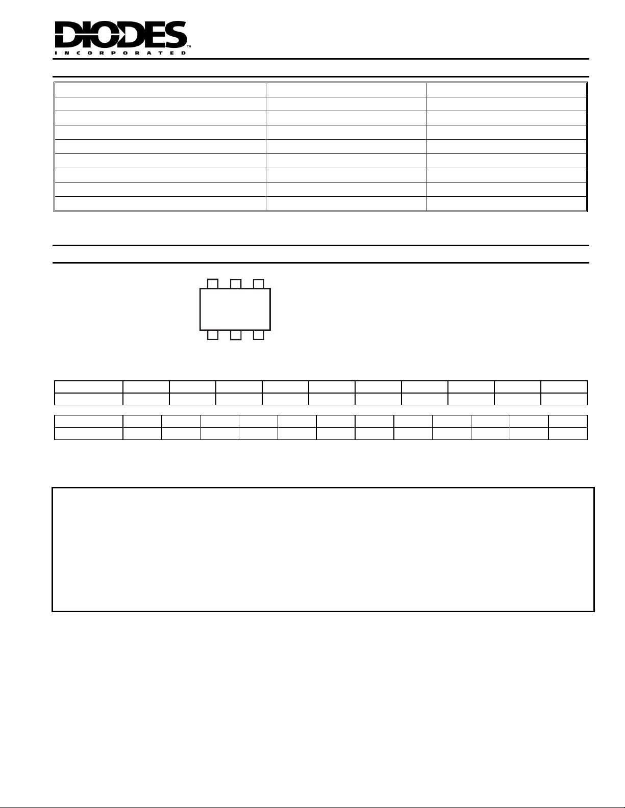
Ordering Information (Note 6)
Device
DDC124EH-7
DDC144EH-7
DDC143EH-7
DDC114YH-7
DDC123JH-7
DDC114EH-7
DDC143TH-7
DDC114TH-7
Notes: 6. For packaging details, go to our website at http://www.diodes.com/datasheets/ap02007.pdf.
Packaging Shipping
SOT-563 3000/Tape & Reel
SOT-563 3000/Tape & Reel
SOT-563 3000/Tape & Reel
SOT-563 3000/Tape & Reel
SOT-563 3000/Tape & Reel
SOT-563 3000/Tape & Reel
SOT-563 3000/Tape & Reel
SOT-563 3000/Tape & Reel
Marking Information
Date Code Key
Year 2003 2004 2005 2006 2007 2008 2009 2010 2011 2012
Code P R S T U V W X Y Z
Month Jan Feb Mar Apr May Jun Jul Aug Sep Oct Nov Dec
Code 1 2 3 4 5 6 7 8 9 O N D
Diodes Incorporated and its subsidiaries reserve the right to make modifications, enhancements, improvements, corrections or other changes
without further notice to any product herein. Diodes Incorporated does not assume any liability arising out of the application or use of any product
described herein; neither does it convey any license under its patent rights, nor the rights of others. The user of products in such applications shall
assume all risks of such use and will agree to hold Diodes Incorporated and all the companies whose products are represented on our website,
harmless against all damages.
Diodes Incorporated products are not authorized for use as critical components in life support devices or systems without the expressed written
approval of the President of Diodes Incorporated.
NXXYM
Nxx = Product Type Marking Code (See Page 1)
YM = Date Code Marking
Y = Year ex: T = 2006
M = Month ex: 9 = September
IMPORTANT NOTICE
LIFE SUPPORT
DS30421 Rev. 4 - 2
4 of 4
www.diodes.com
DDC (xxxx) H
© Diodes Incorporated
 Loading...