

Page 1
Please click here to visit our online spice models database.
General Descriptions
• DDC144NS features discrete dual NPN transistors that
can support continuous maximum current up to 100 mA.
It is suited for applications where the load needs to be
turned on and off using circuits like micro-controllers,
comparators, etc., particularly at a point of load. The
component devices can be used as a part of a circuit or
as a stand alone discrete device.
Features
• Epitaxial Planar Die Construction
• Ideally Suited for Automated Assembly Processes
• Lead Free By Design/RoHS Compliant (Note 1)
• "Green" Device (Note 2)
Mechanical Data
• Case: SOT-363
• Case Material: Molded Plastic. "Green” Molding
Compound. UL Flammability Classification Rating 94V-0
• Moisture Sensitivity: Level 1 per J-STD-020C
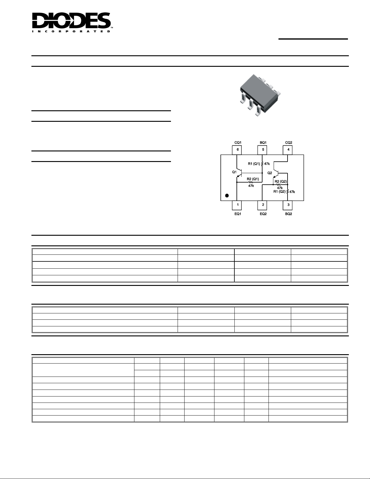
• Terminal Connections: See Figure 2
• Terminals: Finish - Matte Tin annealed over Alloy 42
leadframe. Solderable per MIL-STD-202, Method 208
• Marking Information: See Page 3
• Ordering Information: See Page 3
• Weight: 0.0065 grams (approximate)
DDC144NS
DUAL NPN PRE-BIASED TRANSISTOR
Fig. 1: SOT-363
Fig. 2: Schematic and Pin Configuration
Maximum Ratings, Total Device @T
Characteristic Symbol Value Unit
Power Dissipation (Note 3)
Thermal Resistance, Junction to Ambient Air (Note 3)
Operating and Storage Temperature Range
Collector Current
Maximum Ratings:
Sub-Component Device - Pre-Biased NPN Transistor @T
Characteristic Symbol Value Unit
Supply Voltage
Input Voltage
Output Current Io 100 mA
Electrical Characteristics:
Pre-Biased NPN Transistor @T
Characteristic Symbol Min Typ Max Unit Test Condition
Input Voltage
Output Voltage
Input Current
Output Current
DC Current Gain
Input Resistor (R1) Tolerance
Resistance Ratio Tolerance R2/R1 -20
Gain-Bandwidth Product
Notes: 1. No purposefully added lead.
AP02001, which can be found on our website at http://www.diodes.com/datasheets/ap02001.pdf
DS30747 Rev. 6 - 2
2 . Diodes Inc.'s "Green" policy can be found on our website at http://www.diodes.com/products/lead_free/index.php.
3. Device mounted on FR-4 PCB, 1 inch x 0.85 inch x 0.062 inch; pad layout as shown on page 4 or go to Diodes Inc. suggested pad layout document
A
V
= 25°C unless otherwise specified
A
P
d
R
JA
θ
Tj, T
STG
I
(max)
C
A
V
cc
V
in
= 25°C unless otherwise specified
V
I(off)
V
I(on)
O(on)
I
I
I
O(off)
G
I
Δ R1
f
T
0.5 1.1
⎯
⎯
⎯ ⎯
⎯ ⎯
100
-30
⎯
www.diodes.com
1.5 3 V
0.1 0.3 V
⎯ ⎯ ⎯ V
⎯
⎯
250
1 of 4
⎯
0.18 mA
0.5 uA
+30 %
+20 %
⎯
200 mW
625
-55 to +150
100 mA
= 25°C unless otherwise specified
50 V
-10 to +40 V
V
V
= 5V, IO = 100uA
cc
V
= 0.3V, IO = 2mA
O
I
= 10mA/0.5mA
O/II
V
= 5V
I
Vcc = 50V, VI = 0V
= 5V, IO = 5mA
O
MHz
VCE = 10V, IE = 5mA, f = 100 MHz
°C/W
⎯
⎯
© Diodes Incorporated
°C
DDC144NS
Page 2
P, P
OWER
PATIO
N
C
O
C
TOR CUR
R
N
T
D
C CUR
REN
T GAIN
C
O
CTO
R
OLT
G
C
O
C
T
O
R VOLT
G
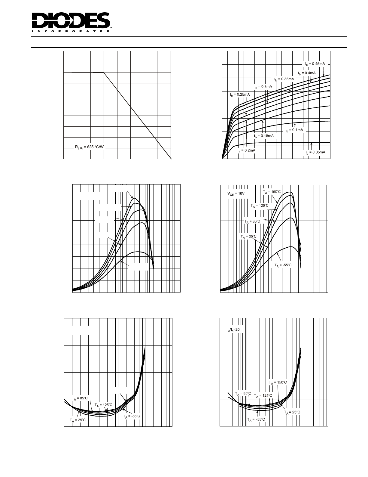
Typical Characteristics of NPN Transistor @ T
250
200
(mW)
150
DISSI
100
D
50
0
-50
450
400
350
300
050100
T , AMBIENT TEMPERATURE ( C)
A
°
Fig. 3 Derating Curve
ο
T = 150
C
A
V = 5V
CE
ο
T = 125
C
A
ο
T = 85
C
A
150
= 25°C unless otherwise specified
A
0.08
0.07
(A)
0.06
E
0.05
0.04
0.03
LLE
0.02
C
I,
0.01
0
0.2
0
0.4 0.6
V , COLLECTOR EMITTER VOLTAGE (V)
CE
0.8
Fig. 4 Typical V vs. I
450
400
350
300
1
1.2
1.4 1.6
CE C
1.8 2
FE
h , DC CURRENT GAIN
100
E(V)
10
A
V
1
LLE
0.1
CE(SAT)
V,
250
200
150
100
50
0
0.1
I/I=10
cb
ο
T = 25
C
A
ο
T = -55
C
A
1
I COLLECTOR CURRENT (mA)
C
10
100
Fig. 5 Typical DC Current Gain
ο
T = 150C
A
1,000
250
200
FE
150
h,
100
50
0
0.1
1
I , COLLECTOR CURRENT (mA)
C
Fig. 6 Typical DC Current Gain
10
100
1,000
100
E (V)
10
A
1
LLE
0.1
CE(SAT)
V,
0.01
0.1
DS30747 Rev. 6 - 2
1100
I , COLLECTOR CURRENT (mA)
C
Fig. 7 Typical V vs. I
10
CE(SAT) C
1,000
www.diodes.com
2 of 4
0.01
0.1 1 10
I , COLLECTOR CURRENT (mA)
C
Fig. 8 Typical V vs. I
100 1,000
CE(SAT) C
DDC144NS
© Diodes Incorporated
Page 3

5
PUT
OLTAG
T
T
R VO
TAG
T
TER
T
TER
E (V)
V
V , IN
V , BASE-EMI
I(ON)
BE(SAT)
2
V = 0.3V
22.5
CE
20
17.5
15
12.5
10
7.5
5
T = -55°C
A
T = 85°C
A
T = 125°C
A
T = 25°C
A
2.5
0
0.1
110
I , OUTPUT CURRENT (mA)
C
Fig. 9 Typical Input Voltage vs. Out put Cur rent
30
27
24
21
18
15
12
9
SATURATION VOLTAGE ( V)
6
3
0
0.1
1
I , COLLECTOR CURRENT (mA)
C
Fig. 11 Typical V vs. I
BE(SAT) C
T = 150°C
A
10
100
100
15
13.5
V = 5V
CE
E (V)
12
10.5
L
9
E
7.5
6
4.5
3
BE(ON)
V , BASE EMI
1.5
0
0.1
T = -55°C
A
1
I , COLLECTOR CURRENT (mA)
C
Fig. 10 Typical V vs. I
T = 85°C
A
T = 25°C
A
BE(ON) C
T = 125°C
A
T = 150°C
A
10 100
30
I/I = 20
27
cb
24
21
18
15
12
9
BE(SAT)
V , BASE-EMI
SATURATION VOLTAGE (V)
6
T = 25°C
A
T = -55°C
A
T = 150°C
A
T = 125°C
A
T = 85°C
A
3
0
0.1 1
I , COLLECTOR CURRENT (mA)
C
Fig. 12 Typical V vs. I
10
BE(SAT) C
100
Ordering Information (Note 4)
Device Packaging Shipping
DDC144NS-7 SOT-363 3000/Tape & Reel
Notes: 4. For packaging details, go to our website at http://www.diodes.com/datasheets/ap02007.pdf.
Marking Information
S20
Date Code Key
Fig. 13
Year 2005 2006 2007 2008 2009 2010 2011 2012
Code S T U V W X Y Z
Month Jan Feb Mar Apr May Jun Jul Aug Sep Oct Nov Dec
Code 1 2 3 4 5 6 7 8 9 O N D
DS30747 Rev. 6 - 2
S20 = Product Type Marking Code,
YM = Date Code Marking
Y = Year, e.g., T = 2006
YM
M = Month, e.g., 9 = September
3 of 4
www.diodes.com
DDC144NS
© Diodes Incorporated
Page 4

Package Outline Dimensions
K
J
A
B C
H
M
F
Fig. 14
L
D
SOT-363
Dim Min Max
A 0.10 0.30
B 1.15 1.35
C 2.00 2.20
D 0.65 Nominal
F 0.30 0.40
H 1.80 2.20
J
K 0.90 1.00
L 0.25 0.40
M 0.10 0.25
α
All Dimensions in mm
0.10
⎯
0° 8°
Suggested Pad Layout
Diodes Incorporated and its subsidiaries reserve the right to make modifications, enhancements, improvements, corrections or other changes
without further notice to any product herein. Diodes Incorporated does not assume any liability arising out of the application or use of any product
described herein; neither does it convey any license under its patent rights, nor the rights of others. The user of products in such applications shall
assume all risks of such use and will agree to hold Diodes Incorporated and all the companies whose products are represented on our website,
harmless against all damages.
Diodes Incorporated products are not authorized for use as critical components in life support devices or systems without the expressed written
approval of the President of Diodes Incorporated.
G
Z
Y
X
EE
Fig. 15
C
IMPORTANT NOTICE
LIFE SUPPORT
Dimensions SOT-363*
Z 2.5
G 1.3
X 0.42
Y 0.6
C 1.9
E 0.65
* Typical dimensions in mm
DS30747 Rev. 6 - 2
4 of 4
www.diodes.com
DDC144NS
© Diodes Incorporated
 Loading...