

Page 1
Features
DDA (xxxx) K
PNP PRE-BIASED SMALL SIGNAL SOT-26
DUAL SURFACE MOUNT TRANSISTOR
Epitaxial Planar Die Construction
·
Complementary NPN Types Available (DDC)
·
Built-In Biasing Resistors
·
Available in Lead Free/RoHS Compliant Version (Note 3)
·
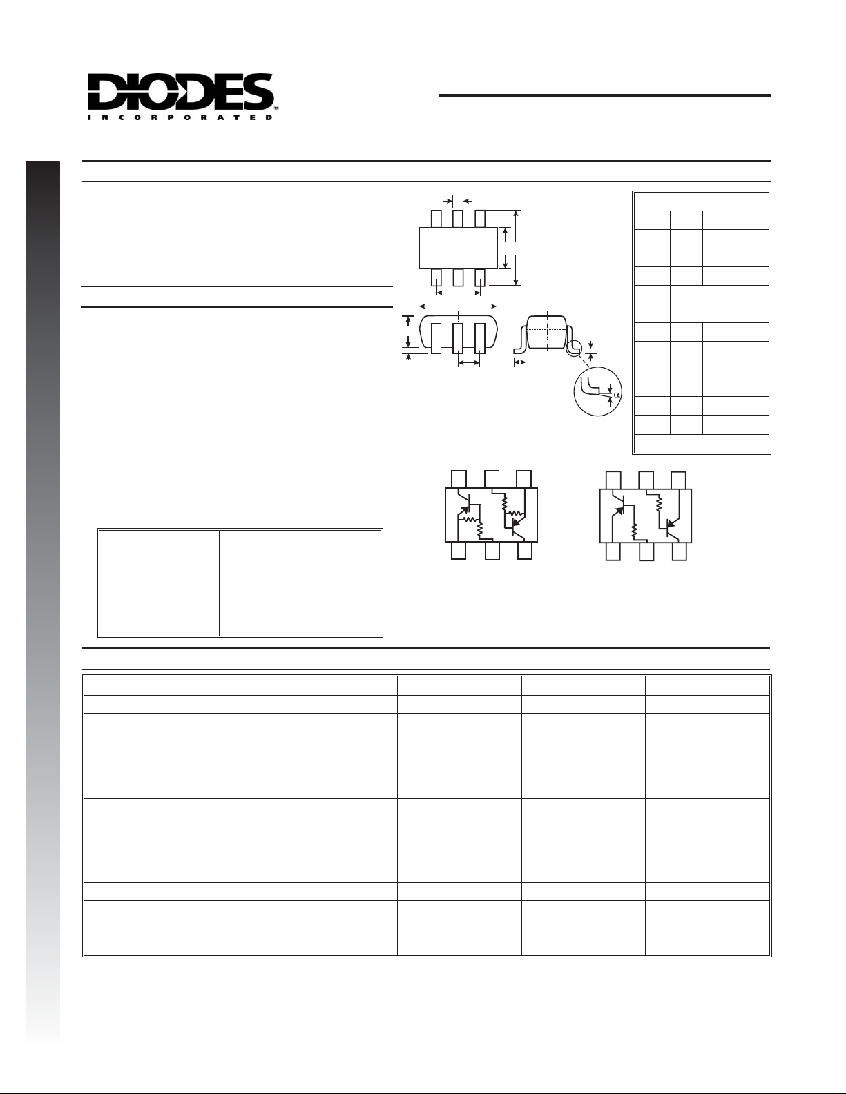
Mechanical Data
Case: SOT-26
·
Case Material: Molded Plastic. UL Flammability
·
NEW PRODUCT
Classification Rating 94V-0
Moisture Sensitivity: Level 1 per J-STD-020C
·
Terminal Connections: See Diagram
·
Terminals: Solderable per MIL-STD-202, Method 208
·
Also Available in Lead Free Plating (Matte Tin Finish
·
annealed over Copper leadframe). Please see Ordering
Information, Note 5, on Page 2
Marking: Date Code and Marking Code (See Diagrams &
·
Page 2)
Ordering Information (See Page 2)
·
Weight: 0.015 grams (approximate)
·
DDA124EK
DDA144EK
DDA114YK
DDA114EK
DDA143TK
DDA114TK
P/N R1 R2 MARKING
DDA123JK
22KW
47KW
10KW
2.2KW
10KW
4.7KW
10KW
22KW
47KW
47KW
47KW
10KW
-
-
P17
P20
P14
P06
P13
P07
P12
K
J
A
PXX YM
G
H
D
6
R
1
PXX YM
C
B
L
5
4
R
R
1
2
R
2
1
3
2
R1, R
2
SCHEMATIC DIAGRAM
SOT-26
Dim Min Max Typ
A
0.35 0.50 0.38
B
1.50 1.70 1.60
C
2.70 3.00 2.80
D
G
M
H
J
K
L
M
a
All Dimensions in mm
6
5
R
1
R
1
2
1
R1Only
0.95
1.90
2.90 3.10 3.00
0.013 0.10 0.05
1.00 1.30 1.10
0.35 0.55 0.40
0.10 0.20 0.15
0° 8°¾
4
3
Maximum Ratings
Supply Voltage, (1) to (6) and (4) to (3)
Input Voltage, (2) to (1) and (5) to (4) DDA124EK
Output Current DDA124EK
Output Current All
Power Dissipation (Total)
Thermal Resistance, Junction to Ambient Air (Note 1)
Operating and Storage and Temperature Range
Note: 1. Mounted on FR4 PC Board with recommended pad layout at http://www.diodes.com/datasheets/ap02001.pdf.
2. 200mW per element must not be exceeded.
3. No purposefully added lead.
@ TA= 25°C unless otherwise specified
Characteristic Symbol Value Unit
DDA144EK
DDA114YK
DDA123JK
DDA114EK
DDA143TK
DDA114TK
DDA144EK
DDA114YK
DDA123JK
DDA114EK
DDA143TK
DDA114TK
V
I
C
R
T
j,TSTG
CC
V
IN
I
O
(Max)
P
d
qJA
50 V
+10 to -40
+10 to -40
+6 to -40
+5 to -12
+10 to -40
+5 Vmax
+5 Vmax
-30
-30
-70
-100
-50
-100
-100
-100 mA
300
416.7 °C/W
-55 to +150 °C
mA
mW
V
DS30349 Rev. 5 - 2 1 of 6 DDA (xxxx) K
www.diodes.com
ã Diodes Incorporated
Page 2
Electrical Characteristics
@ TA= 25°C unless otherwise specified
Characteristic (DDA143TK & DDA114TK only) Symbol Min Typ Max Unit Test Condition
Collector-Base Breakdown Voltage
Collector-Emitter Breakdown Voltage
Emitter-Base Breakdown Voltage
Collector Cutoff Current
Emitter Cutoff Current
Collector-Emitter Saturation Voltage
DC Current Transfer Ratio
NEW PRODUCT
Input Resistor (R1) Tolerance
Gain-Bandwidth Product*
BV
BV
BV
I
I
V
CE(sat)
h
DR
CBO
CEO
EBO
CBO
EBO
FE
f
T
-50 ¾¾ V
-50 ¾¾ V
-5 ¾¾ V
¾¾-0.5 mA
¾¾-0.5 mA
¾¾-0.3 V
100 250 600 --
-30 ¾ +30 %
1
¾ 250 ¾ MHz
= -2.5mA /- 0.25mA DDA143TK
I
C/IB
I
= -1mA /- 0.1mA DDA114TK
C/IB
I
= -10V, IE= 5mA, f = 100MHz
V
CE
Characteristic Symbol Min Typ Max Unit Test Condition
Input Voltage
Output Voltage
Input Current
Output Current
DC Current Gain
Input Resistor (R1) Tolerance
Resistance Ratio Tolerance
Gain-Bandwidth Product*
DDA124EK
DDA144EK
DDA114YK
DDA123JK
DDA114EK
DDA124EK
DDA144EK
DDA114YK
DDA123JK
DDA114EK
DDA124EK
DDA144EK
DDA114YK
DDA123JK
DDA114EK
DDA124EK
DDA144EK
DDA114YK
DDA123JK
DDA114EK
DDA124EK
DDA144EK
DDA114YK
DDA123JK
DDA114EK
V
V
V
I
R
l(off)
l(on)
O(on)
I
l
O(off)
G
DR
2/R1
f
T
-0.5
-0.5
-0.3
-0.5
-0.5
¾
¾ -0.1
¾¾
¾¾-0.5 mA
56
68
l
1
68
80
30
-30 ¾ +30 %
-20 ¾ +20 %
¾ 250 ¾ MHz
-1.1
-1.1
¾
¾
¾
-1.1
-1.9
-1.9
¾
¾
-1.9
-0.36
-0.18
-0.88
-0.88
-3.0
-3.0
-1.4
-1.1
-3.0
-0.3
-3.6
V
V
mA
¾¾¾
V
CC
V
= -0.3, IO= -5mA
O
V
= -0.3, IO= -2mA
O
V
= -0.3, IO= -1mA
O
V
= -0.3, IO= -5mA
O
V
= -0.3, IO= -10mA
O
= -10mA /- 0.5mA
I
O/Il
I
= -10mA /- 0.5mA
O/Il
I
= -5mA / -0.25mA
O/Il
I
= -5mA / -0.25mA
O/Il
I
= -10mA / -0.5mA
O/Il
= -5V
V
I
V
CC
= -5V, IO= -5mA
V
O
V
= -5V, IO= -5mA
O
V
= -5V, IO= -10mA
O
V
= -5V, IO= -10mA
O
V
= -5V, IO= -5mA
O
V
CE
f = 100MHz
* Transistor - For Reference Only
= -50mA
I
C
= -1mA
I
C
= -50mA
I
E
= -50V
V
CB
= -4V
V
EB
= -1mA, VCE= -5V
C
¾
= -5V, IO= -100mA
= 50V, VI= 0V
¾
¾
= -10V, IE= -5mA,
Ordering Information
Device
DDA124EK-7
DDA144EK-7
DDA114YK-7
DDA123JK-7
DDA114EK-7
DDA143TK-7
DDA114TK-7
Notes: 4. For Packaging Details, go to our website at http://www.diodes.com/datasheets/ap02007.pdf.
5. For Lead Free/RoHS Compliant version part numbers, please add "-F" suffix to the part numbers above. Example: DDA114TK-7-F.
(Note 4)
Packaging Shipping
SOT-26 3000/Tape & Reel
SOT-26 3000/Tape & Reel
SOT-26 3000/Tape & Reel
SOT-26 3000/Tape & Reel
SOT-26 3000/Tape & Reel
SOT-26 3000/Tape & Reel
SOT-26 3000/Tape & Reel
DS30349 Rev. 5 - 2 2 of 6 DDA (xxxx) K
www.diodes.com
Page 3

Marking Information
Date Code Key
Year 2006
Code
NEW PRODUCT
Month Jan Feb Mar Apr May Jun Jul
Code
PXX YM
PXX YM
2007 2008
T
1234567
UV
PXX = Product Type Marking Code
See Sheet 1 Diagrams
YM = Date Code Marking
Y = Year ex: T = 2006
M = Month ex: 9 = September
2009 2010 2011
WXY
Aug Sep Oct Nov Dec
2012
Z
89 OND
DS30349 Rev. 5 - 2 3 of 6 DDA (xxxx) K
www.diodes.com
Page 4

10
g
100
g
C
C
C
1000
1
(
250
200
g
150
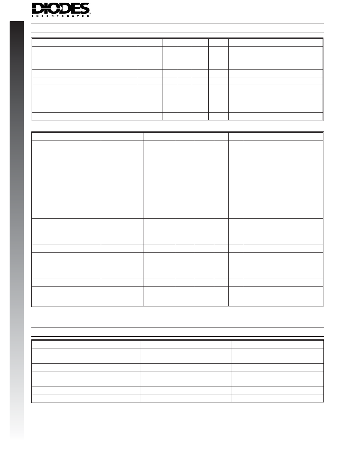
TYPICAL CURVES - DDA123JK
ONE SECTION
0.1
I/I =10
CB
75 C°
-25 C°
25 C°
NEW PRODUCT
D
P , POWER DISSIPATION (mW)
100
50
0
100
FE
h , DC CURRENT GAIN
10
-50
V=10V
CE
0 50 100 150
T , AMBIENT TEMPERATURE ( C)
A
Fi
. 1 DeratingCurve
75 C°
-25 C°
°
25 C°
1 10 100
I , COLLECTOR CURRENT (mA)
C
Fig. 3 DC Current Gain
ITANCE (pF)
APA
,
OB
12
10
0.01
CE(SAT)
V , COLLECTOR EMITTER VOLTAGE (V)
0.001
10
0
I , COLLECTOR CURRENT (mA)
C
20
Fig. 2
30
V vs. I
CE
SAT)C
40
50
f = 1MHz
8
6
4
2
0
0
5
10
V , REVERSE BIAS VOLTAGE (V)
R
15
20
25
30
Fig. 4 Output Capacitance
75°C
10
25°C
-25°C
1
V=5V
O
V = 0.2V
O
-25°C
1
75 C°
0.1
in
0.01
C
I , COLLECTOR CURRENT (mA)
0.001
1
0
234
V , INPUT VOLTAGE (V)
in
. 5 Collector Current Vs. Input Voltage
Fi
5
67
89
10
V , INPUT VOLTAGE (V)
25°C
0.1
01020304050
I , COLLECTOR CURRENT (mA)
C
Fi
. 6 Input Voltage vs. Collector Current
DS30349 Rev. 5 - 2 4 of 6 DDA (xxxx) K
www.diodes.com
Page 5

10
g
100
g
C
C
C
1000
1
(
250
200
g
150
TYPICAL CURVES - DDA114TK
ONE SECTION
I/I =10
0.1
CB
25 C°
-25 C°
75 C°
D
P , POWER DISSIPATION (mW)
100
50
NEW PRODUCT
0
100
10
FE
h , DC CURRENT GAIN
1
-50
0 50 100 150
T , AMBIENT TEMPERATURE ( C)
A
Fi
. 1 DeratingCurve
75 C°
-25 C°
25 C°
°
V=10V
CE
1 10 100
I , COLLECTOR CURRENT (mA)
C
Fig. 3 DC Current Gain
ITANCE (pF)
APA
,
OB
12
10
0.01
CE(SAT)
V , COLLECTOR EMITTER VOLTAGE (V)
0.001
10
0
I , COLLECTOR CURRENT (mA)
C
20
Fig. 2
30
V vs. I
CE
SAT)C
40
50
f=1MHz
8
6
4
2
0
0
5
V , REVERSE BIAS VOLTAGE (V)
10
R
15
20
25
30
Fig. 4 Output Capacitance
75°C
25°C
V = 0.2V
O
10
-25°C
C
I , COLLECTOR CURRENT (mA)
0.1
0.01
1
in
V , INPUT VOLTAGE (V)
-25°C
1
75 C°
25°C
0.001
01234
. 5 Collector Current Vs. Input Voltage
Fi
67
5
V , INPUT VOLTAGE (V)
in
89
10
1
01020304050
I , COLLECTOR CURRENT (mA)
C
Fi
. 6 Input Voltage vs. Collector Current
DS30349 Rev. 5 - 2 5 of 6 DDA (xxxx) K
www.diodes.com
Page 6

IMPORTANT NOTICE
Diodes Incorporatedand its subsidiaries reserve the right to make modifications, enhancements, improvements, corrections or other changes without further
notice to any product herein. Diodes Incorporated does not assume any liability arising out of the application or use of any product described herein; neither
does it convey any license under its patent rights, nor the rights of others. The user of products in such applications shall assume all risks of such use and will
agree to hold Diodes Incorporated and allthe companies whose products are represented onour website, harmlessagainst all damages.
LIFE SUPPORT
Diodes Incorporated products are not authorized for use as criticalcomponents in lifesupport devices or systems without the expressedwritten approval ofthe
President of Diodes Incorporated.
NEW PRODUCT
DS30349 Rev. 5 - 2 6 of 6 DDA (xxxx) K
www.diodes.com
 Loading...