

Page 1
)
θ
Please click here to visit our online spice models database.
General Descriptions
• DCX100NS is best suited for applications where the load
needs to be turned on and off using control circuits like
micro-controllers, comparators etc. particularly at a point
of load. It features a discrete PNP pass transistor which
can support continuous maximum current up to 100 mA. It
also contains an NPN transistor which can be used as a
control switch and can also be biased using higher
supply. The component devices can be used as part of a
circuit or as stand alone discrete devices.
Features
• Built in Biasing Resistors
• Epitaxial Planar Die Construction
• Lead Free By Design/ROHS Compliant (Note 1)
• "Green" Device (Note 2)
• Ideally Suited for Automated Assembly Processes
DCX100NS
100mA DUAL PRE-BIASED TRANSISTORS
SOT-563
Mechanical Data
• Case: SOT-563
• Case Material: Molded Plastic. "Green” Molding
Compound. UL Flammability Classification Rating 94V-0
• Moisture Sensitivity: Level 1 per J-STD-020
• Terminal Connections: See Diagram
• Terminals: Finish - Matte Tin annealed over Copper
leadframe. Solderable per MIL-STD-202, Method 208
• Marking Information: See Page 5
• Ordering Information: See Page 5
• Weight: 0.0035 grams (approximate)
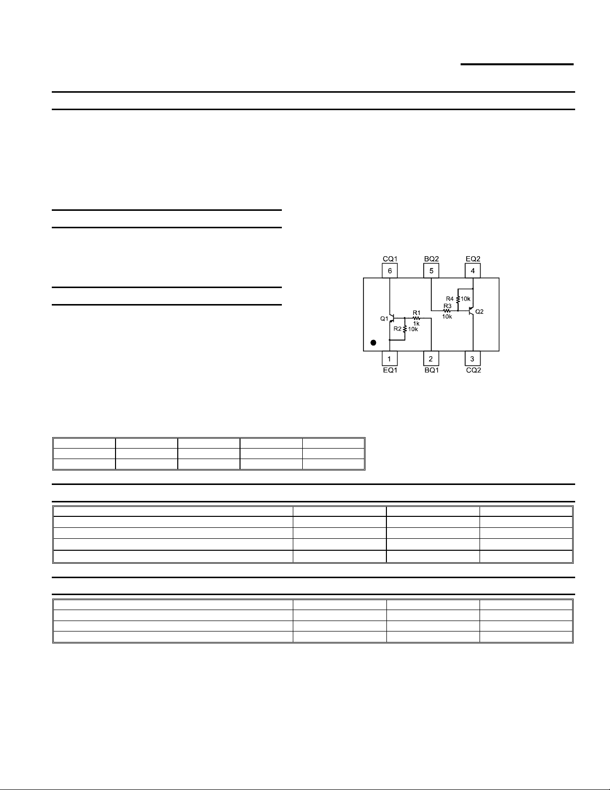
Reference Device Type R1 (NOM)
Q1 PNP
Q2 NPN
1KΩ
⎯
Maximum Ratings: Total Device @T
Characteristic Symbol Value Unit
Power Dissipation (Note 3)
Collector Current (using PNP as Pass Transistor)
Thermal Resistance, Junction to Ambient Air (Note 3)
Operating and Storage Junction Temperature Range
R2 (NOM) R3, R4 (NOM)
10KΩ
⎯
= 25°C unless otherwise specified
A
⎯
10KΩ
PD
I
C(max
R
TJ, T
JA
STG
Schematic and Pin Configuration
150 mW
100 mA
833
-55 to +150 °C
°C/W
Sub-Component Device - Pre-Biased PNP Transistor @T
Supply Voltage
Input Voltage
Output Current
Notes: 1. No purposefully added lead.
our website at http://www.diodes.com/datasheets/ap02001.pdf.
DS30761 Rev. 6 - 2
2. Diodes Inc.'s "Green" policy can be found on our website at http:/www.diodes.com/products/lead_free/index.php.
3. Device mounted on FR-4 PCB, 1 inch x 0.85 inch x 0.062 inch; please see page 6 or as per Diodes Inc. suggested pad layout document AP02001 on
Characteristic Symbol Value Unit
Vcc
Vin
Ic
1 of 6
www.diodes.com
= 25°C unless otherwise specified
A
-50 V
+5 to -10 V
-100 mA
© Diodes Incorporated
DCX100NS
Page 2
)
)
)
)
)
)
)
)
P, P
OWER
PATIO
N
Sub-Component Device - Pre-Biased NPN Transistor @T
Characteristic Symbol Value Unit
Supply Voltage
Input Voltage
Output Current
Vcc
Vin
IO
= 25°C unless otherwise specified
A
50 V
-10 to +40 V
50 mA
Electrical Characteristics: Pre-Biased PNP Transistor @T
= 25°C unless otherwise specified
A
Characteristic Symbol Min Typ Max Unit Test Condition
Input Voltage
Output Voltage
Input Current
Output Current
DC Current Gain
Input Resistor Tolerance
-0.3
V
I(off
V
⎯ ⎯
I(on
V
⎯
O(on
II ⎯ ⎯
⎯ ⎯
I
O(off
G
I
Δ R1
33
-30
⎯ ⎯
-3.0 V
0.1 -0.3 V
-7.2 mA
-0.5 uA
⎯ ⎯ ⎯
⎯
+30 %
Resistance Ratio Tolerance R2/R1 0.8 1 1.2 %
Gain-Bandwidth Product
Electrical Characteristics: Pre-Biased NPN Transistor @T
f
⎯
T
250
⎯
A
MHz
= 25°C unless otherwise specified
Characteristic Symbol Min Typ Max Unit Test Condition
Input Voltage
Output Voltage
Input Current
Output Current
DC Current Gain
Input Resistor Tolerance
V
I(off
V
⎯
I(on
V
O(on
I
I
I
⎯ ⎯
O(off
G
I
ΔR1
0.5 1.18
⎯
⎯ ⎯
30
-30
⎯
1.85 3 V
0.1 0.3 V
0.88 mA
0.5 uA
⎯ ⎯ ⎯ VO = 5V, IO = 5mA
⎯
+30 %
Resistor Ratio Tolerance R2/R1 0.8 1 1.2
Gain-Bandwidth Product
f
⎯
T
250
⎯
V
V
= -5V, IO = -100uA
CC
VO = -0.3V, IO = -20mA
I
= -10mA /-0.5mA
O/II
VI = -5V
VCC = -50V, VI = 0V
VO = -5V, IO = -5mA
= -10V, IE = -5mA,
V
CE
f = 100 MHz
V
VCC = 5V, IO = 100uA
VO = 0.3V, IO = 10mA
IO/II = 10mA / 0.5mA
VI = 5V
VCC = 50V, VI = 0V
⎯ ⎯
V
= 10V, IE = 5mA,
MHz
CE
f = 100 MHz
⎯
⎯
⎯
Typical Characteristics @T
= 25°C unless otherwise specified
A
250
200
(mW)
150
DISSI
100
D
50
0
-50
DS30761 Rev. 6 - 2
050100150
T , AMBIENT TEMPERATURE ( C)
A
°
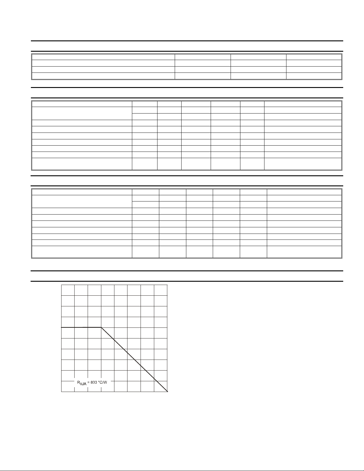
Fig. 1 Power Derating Curve (Total Device)
2 of 6
www.diodes.com
DCX100NS
© Diodes Incorporated
Page 3
C
O
C
TOR CUR
R
T
C CUR
RENT G
C
O
CTO
R
T
TER
PUT VO
TAG
Characteristics Curves of PNP Transistor (Q1) @T
AIN
FE
h, D
300
250
200
150
100
50
100
0.2
0.18
0.16
(A)
0.14
EN
0.12
0.1
0.08
LLE
0.06
C
0.04
I,
0.02
0
0
0.2 0.4 0.6 0.8
V
, COLLECTOR EMITTER VOLTAGE (V)
CE
1
1.2 1.4
1.6
1.8
2
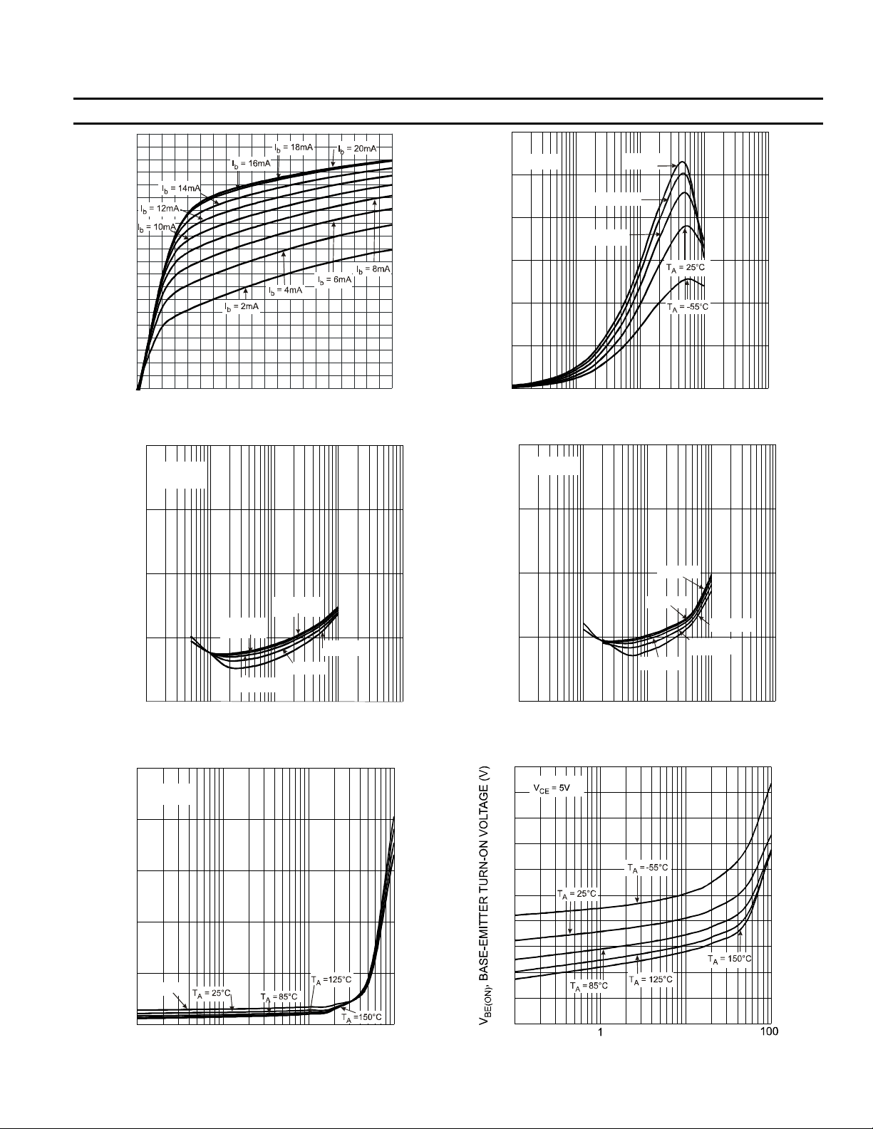
Fig. 2 Typical Collector Current vs. Collector-Emitter Voltage
100
I/I=10
cb
10
= 25°C unless otherwise specified
A
T = 150C
°
A
°
10
100 1,000
0
0.1
V = 5V
CE
T = 125C
A
T = 85C
°
A
1
I , COLLECTOR CURRENT (mA)
C
Fig. 3 Typical DC Current Gain vs. Collector Current
I/I=20
cb
10
1
T = 150 C
°
A
T = 125 C
°
0.1
SATURATION VOL TAGE (V)
CE(SAT)
V , COLLECTOR-EMITTER
0.01
0.1 1 10 100
A
T = 25C
T = 85C
A
I , COLLECTOR CURRENT (mA)
C
A
°
Fig. 4 Typical Collector-Emitter Saturation Voltage
vs. Collector Current
15
V = 0.3V
CE
12
E (V)
9
L
6
IN
3
T =-55°C
A
T = -55C
A
°
-EMI
1
T =150°C
A
LLE
T =125°C
A
T =-55°C
0.1
SATURATION VOLTAGE (V)
°
CE(SAT)
V,
T =85°C
A
A
T = 25°C
A
0.01
1,000
0.1
1
I , COLLECTOR CURRENT (mA)
C
10 100 1,000
Fig. 5 Typical Collector-Emitter Saturation Voltage
vs. Collector Current
2
1.8
1.6
1.4
1.2
1
0.8
0.6
0.4
0.2
0
0.1
1100
I , COLLECTOR CURRENT (mA)
C
10
Fig. 6 Typical Input Voltage vs. Collector Current
DS30761 Rev. 6 - 2
3 of 6
www.diodes.com
0
0.1
I , COLLECTOR CURRENT (mA)
C
10
Fig. 7 Typical Base-Emitter Turn-On Voltage vs. Collector Current
DCX100NS
© Diodes Incorporated
Page 4

15
12
8
7
6
4
6
3
3
0
I , COLLECTOR CURRENT (mA)
C
1
Fig. 8 Typical Base-Em it t er Saturatio n Voltage
vs. Collect or Current
Characteristics Curves of NPN Transistor (Q2) @T
0.1
0.09
)
A
(
0.08
T
N
0.07
E
R
R
U
0.06
C
R
0.05
O
T
C
E
0.04
L
L
O
0.03
C
,
C
I
0.02
0.01
0
0 0.4 0.8 1.2 1.6 2
V , COLLECTOR-EMITTER VOLTAGE (V)
Fig. 10 Typical Collector Current vs. Collector-Emitter Voltage
CE
100
2
10
I , COLLECTOR CURRENT (mA)
C
Fig. 9 Typical Base-Emitter Saturation Voltage
vs. Collector Current
= 25°C unless otherwise specified
A
300
250
200
150
100
50
0
0.1
I , COLLECTOR CURRENT (mA)
C
10
Fig. 11 T yp ical DC Current Gain vs. Collector Current
100
I/I=20
cb
10
1
0.1
SATURA TION VOL TAGE (V)
CE(SAT)
V , COLLECTOR - EMITTE R
0.01
0.1 1 10
Fig. 12 Typical Collector-Emitter Saturation Voltage
DS30761 Rev. 6 - 2
T = 150C
°
A
T = 125C
°
A
T = 85C
°
A
T = 25C
°
A
T = -55C
°
A
I , COLLECTOR CURRENT (mA)
C
100
vs. Collector Current
1,000
4 of 6
www.diodes.com
10
1
0.1
SATURATION VOLT AGE (V)
CE(SAT)
V , COLLECTOR-EMITTER
0.01
0.1 1 10 100 1,000
I , COLLECTOR CURRENT (mA)
C
Fig. 13 Typical Collector-Emitter Saturation Voltage
vs. Collector Current
DCX100NS
© Diodes Incorporated
Page 5

25
25
V = 5V
CE
20
15
10
INPUT VOLTAGE (V)
5
0
0.1
110
I , COLLECTOR CURRENT (mA)
C
100
Fig. 14 Typical Input volt age vs. Outp ut Cu r r ent
30
I/I=10
cb
24
18
T = -55C
°
A
12
T = 25C
°
A
T = 85C
°
6
0
0.1
BE(SAT)
V , BASE-EMITTER SATURATION VOLT AGE (V)
I , COLLECTOR CURRENT (mA)
C
A
T = 125C
°
A
T = 150C
°
A
110
100
Fig. 16 Typical Base-Emitter Saturation Voltage
vs. Collector Current
20
15
T = 150C
A
T = 125C
°
A
°
10
T = 85C
°
A
5
T = -55C
A
BE(ON)
V , BASE-EMITTER TURN-ON VOLT AGE (V)
0
0.1
I , COLLECTOR CURRENT (mA)
C
110
°
T = 25C
°
A
100
Fig. 15 Typical Base-Emitter Turn-On Voltage vs. Collector Current
30
I/I = 20
cb
24
18
12
T = -55C
°
T = 25C
°
A
A
T = 85C
A
T = 150C
A
T = 125C
A
°
°
°
110
100
6
0
0.1
BE(SAT)
V , BASE-EMITTER SATURATION VOLTAGE (V)
I , COLLECTOR CURRENT (mA)
C
Fig. 17 Typical Base-Emitter Saturation Voltage
vs. Collector Current
Ordering Information (Note 4)
Device
DCX100NS-7
Notes: 4. For packaging details, please see page 6 or go to our website at http://www.diodes.com/datasheets/ap02007.pdf.
Packaging Shipping
SOT-563 3000/Tape & Reel
Marking Information
C01 YM
C01 = Product Type Marking Code
YM = Date Code Marking
Y = Year e.g., T = 2006
M = Month e.g., 9 = September
Date Code Key
Year 2005 2006 2007 2008 2009 2010 2011 2012
Code S T U V W X Y Z
Month Jan Feb Mar Apr May Jun Jul Aug Sep Oct Nov Dec
Code 1 2 3 4 5 6 7 8 9 O N D
DS30761 Rev. 6 - 2
5 of 6
www.diodes.com
DCX100NS
© Diodes Incorporated
Page 6

Package Outline Dimensions
K
A
Dim Min Max Typ
B
C
D
G
M
H
L
SOT-563
A 0.15 0.30 0.20
B 1.10 1.25 1.20
C 1.55 1.70 1.60
D - - 0.50
G 0.90 1.10 1.00
H 1.50 1.70 1.60
K 0.55 0.60 0.60
L 0.10 0.30 0.20
M 0.10 0.18 0.11
All Dimensions in mm
Suggested Pad Layout
G
Z
Y
X
C2
C2
C1
Dimensions Value (in mm)
Z 2.2
G 1.2
X 0.375
Y 0.5
C1 1.7
C2 0.5
DS30761 Rev. 6 - 2
6 of 6
www.diodes.com
DCX100NS
© Diodes Incorporated
Page 7

DIODES INCORPORATED MAKES NO WARRANTY OF ANY KIND, EXPRESS OR IMPLIED, WITH REGARDS TO THIS DOCUMENT,
INCLUDING, BUT NOT LIMITED TO, THE IMPLIED WARRANTIES OF MERCHANTABILITY AND FITNESS FOR A PARTICULAR PURPOSE
(AND THEIR EQUIVALENTS UNDER THE LAWS OF ANY JURISDICTION).
Diodes Incorporated and its subsidiaries reserve the right to make modifications, enhancements, improvements, corrections or other changes
without further notice to this document and any product described herein. Diodes Incorporated does not assume any liability arising out of the
application or use of this document or any product described herein; neither does Diodes Incorporated convey any license under its patent or
trademark rights, nor the rights of others. Any Customer or user of this document or products described herein in such applications shall assume
all risks of such use and will agree to hold Diodes Incorporated and all the companies whose products are represented on Diodes Incorporated
website, harmless against all damages.
Diodes Incorporated does not warrant or accept any liability whatsoever in respect of any products purchased through unauthorized sales channel.
Should Customers purchase or use Diodes Incorporated products for any unintended or unauthorize d application, Customers shall indemnify and
hold Diodes Incorporated and its representatives harmless against all claims, damages, expenses, and attorney fees arising out of, directly or
indirectly, any claim of personal injury or death associated with such unintended or unauthorized application.
Products described herein may be covered by one or more United States, international or foreign patents pending. Product names and markings
noted herein may also be covered by one or more United States, international or foreign trademarks.
Diodes Incorporated products are specifically not authorized for use as critical components in life support devices or systems without the express
written approval of the Chief Executive Officer of Diodes Incorporated. As used herein:
A. Life support devices or systems are devices or systems which:
1. are intended to implant into the body, or
2. support or sustain life and whose failure to perform when properly used in accordance with instructions for use provided in the
labeling can be reasonably expected to result in significant injury to the user.
B. A critical component is any component in a life support device or system whose failure to perform can be reasonably expected to cause the
failure of the life support device or to affect its safety or effectiveness.
Customers represent that they have all necessary expertise in the safety and regulatory ramifications of their life support devices or systems, and
acknowledge and agree that they are solely responsible for all legal, regulatory and safety-related requirements concerning their products and any
use of Diodes Incorporated products in such safety-critical, life support devices or systems, notwithstanding any devices- or systems-related
information or support that may be provided by Diodes Incorporated. Further, Customers must fully indemnify Diodes Incorporated and its
representatives against any damages arising out of the use of Diodes Incorporated products in such safety-critical, life support devices or systems.
Copyright © 2009, Diodes Incorporated
www.diodes.com
IMPORTANT NOTICE
LIFE SUPPORT
DS30761 Rev. 6 - 2
7 of 6
www.diodes.com
DCX100NS
© Diodes Incorporated
 Loading...