Diodes D5V0F4U6SO User Manual

4 CHANNEL LOW CAPACITANCE TVS DIODE ARRAY
Features
IEC 61000-4-2 (ESD): Air – ±15kV, Contact – ±8kV
4 Channels of ESD protection
Low Channel Input Capacitance of 0.5pF Typical
Typically Used at High Speed Ports such as USB 2.0, USB3.0,
IEEE1394, Serial ATA, DVI, HDMI, PCI
Totally Lead-Free & Fully RoHS Compliant (Notes 1 & 2)
Halogen and Antimony Free. “Green” Device (Note 3)
NEW PRODUCT
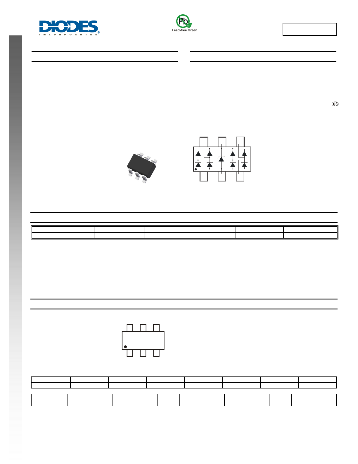
SOT26
Top View
Mechanical Data
Case: SOT26
Case Material: Molded Plastic, “Green” Molding Compound. UL
Flammability Classification Rating 94V-0
Moisture Sensitivity: Level 1 per J-STD-020
Terminals: Matte Tin Finish annealed over Copper leadframe
(Lead Free Plating). Solderable per MIL-STD-202, Method 208
Weight: 0.016 grams (approximate)
CH 4
65 4
12 3
CH 1
Device Schematic
V
DD
GND
CH 3
CH 2
D5V0F4U6SO
Ordering Information (Note 4)
Product Compliance Marking Reel size(inches) Tape width(mm) Quantity per reel
D5V0F4U6SO-7 Standard TV7 7 8 3,000/Tape & Reel
Notes: 1. No purposely added lead. Fully EU Directive 2002/95/EC (RoHS) & 2011/65/EU (RoHS 2) compliant.
2. See http://www.diodes.com/quality/lead_free.html for more information about Diodes Incorporated’s definitions of Halogen- and Antimony-free, "Green"
and Lead-free.
3. Halogen- and Antimony-free "Green” products are defined as those which contain <900ppm bromine, <900ppm chlorine (<1500ppm total Br + Cl) and
<1000ppm antimony compounds.
4. For packaging details, go to our website at http://www.diodes.com/products/packages.html.
Marking Information
Date Code Key
Year 2013 2014 2015 2016 2017 2018 2019
Code A B C D E F G
Month Jan Feb Mar Apr May Jun Jul Aug Sep Oct Nov Dec
Code 1 2 3 4 5 6 7 8 9 O N D
TV7
YM
D5V0F4U6SO
Document number: DS35472 Rev. 4 - 2
TV7 = Product Type Marking Code
YM = Date Code Marking
Y = Year (ex: A = 2013)
M = Month (ex: 9 = September)
1 of 4
www.diodes.com
July 2013
© Diodes Incorporated

P
P
O
R
P
TIO
P
P
U
R
T
G
O
D5V0F4U6SO
Maximum Ratings (@T
= +25°C, unless otherwise specified.)
A
Characteristic Symbol Value Unit Conditions
Peak Pulse Current
ESD Protection – Contact Discharge
ESD Protection – Air Discharge
I
PP
V
ESD_Contact
V
ESD_Air
3.0 A
±8 kV
±15 kV
8/20µs, Per Figure 3
Standard IEC 61000-4-2
Standard IEC 61000-4-2
Thermal Characteristics
Characteristic Symbol Value Unit
Power Dissipation (Note 5)
Thermal Resistance, Junction to Ambient (Note 5)
Operating and Storage Temperature Range
P
D
R
θJA
T
, T
J
STG
300 mW
417 °C/W
-65 to +150 °C
NEW PRODUCT
Electrical Characteristics (@T
Characteristic Symbol Min Typ Max Unit Test Conditions
Reverse Working Voltage
Reverse Current (Note 6)
Reverse Breakdown Voltage
Reverse Clamping Voltage, Positive Transients
(Note 7)
Dynamic Resistance
Capacitance (Note 8)
Notes: 5. Device mounted on FR-4 PCB pad layout (2oz copper) as shown on Diodes, Inc. suggested pad layout AP02001, which can be found on our website at
http://www.diodes.com.
6. Short duration pulse test used to minimize self-heating effect.
7. Clamping voltage value is based on an 8x20µs peak pulse current (I
8. Measured from any CH to GND.
9. For information on the impact of Diodes' USB 2.0 compatible ESD protectors on signal integrity including eye diagram plots, please refer to AN77 at the
following URL:http://www.diodes.com/destools/appnote_dnote.html.
300
= +25°C, unless otherwise specified.)
A
V
R
RWM
I
V
V
DYN
C
R
BR
CL
T
— — 5.5 V —
— — 200 nA
6.0 — — V
— 10 12 V
— 1.0 — Ω
— 0.4 0.65 pF
— 0.5 — pF
) waveform.
PP
100
VR = 5.5V
IR = 1mA
IPP = 1A, tp = 8/20μs
IR = 1A, tp = 8/20μs
V
= 2.5V, f = 1MHz
R
V
= 0V, f = 1MHz
R
Note 5
250
N (mW)
200
A
150
F
%
IN
A
75
50
DISSI
LSE DE
WE
100
,
D
EAK
25
PEAK POWER OR CURRENT
50
0
0125175
25 10050 75 150
T , AMBIENT TEMPERATURE ( C)
A
°
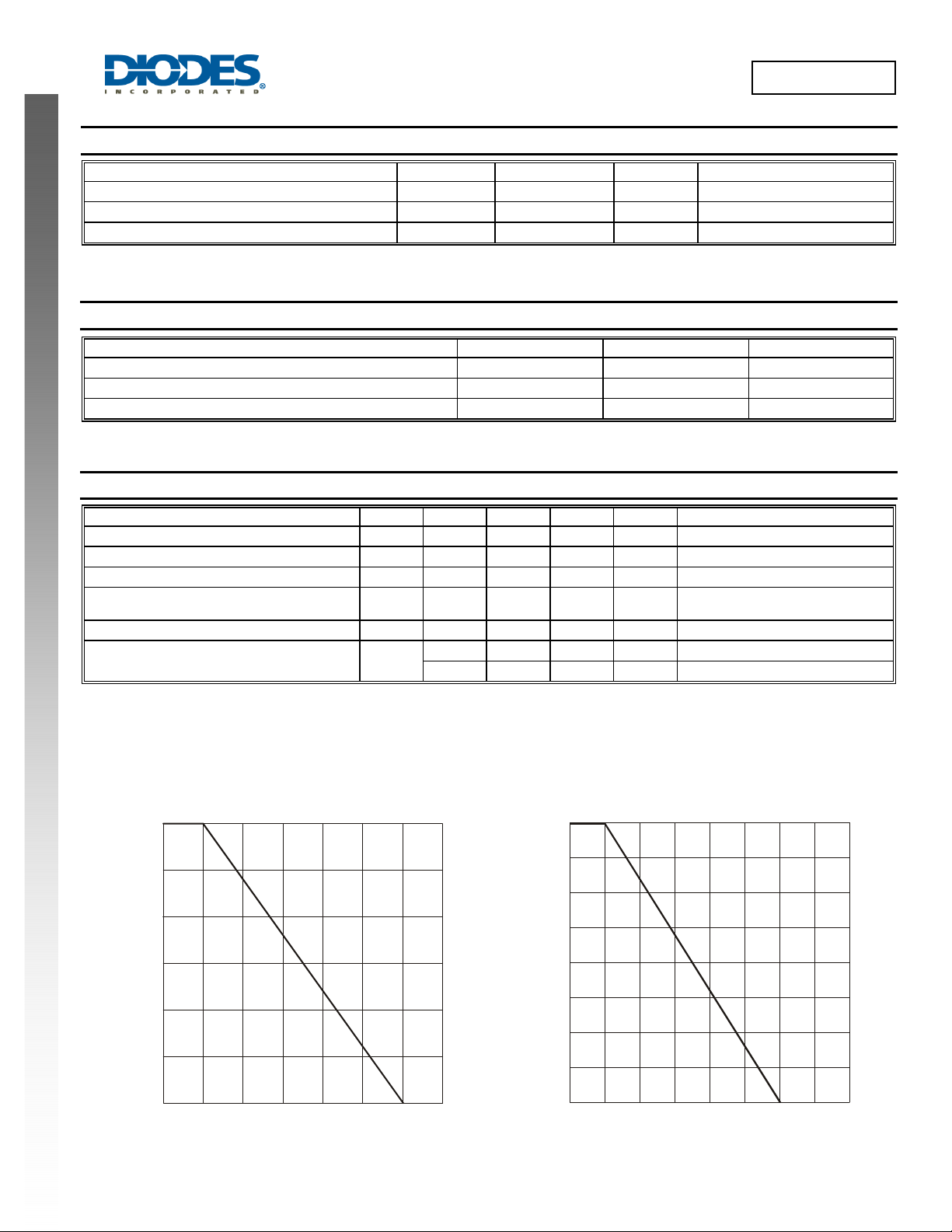
Figure 1 Power Derating Curve
D5V0F4U6SO
Document number: DS35472 Rev. 4 - 2
2 of 4
www.diodes.com
0
0125175
25 10050 75 150
T , AMBIENT TEMPERATURE ( C)
A
°
200
Figure 2 Pulse Derating Curve
July 2013
© Diodes Incorporated
 Loading...