

Page 1
Features
• 400mW Power Dissipation on FR-4 PCB
• Very Tight Tolerance on V
• Ideally Suited for Automated Assembly Processes
• Totally Lead-Free & Fully RoHS Compliant (Notes 1 & 2)
• Halogen and Antimony Free. “Green” Device (Note 3)
NEW PRODUCT NEW PRODUCT
Z
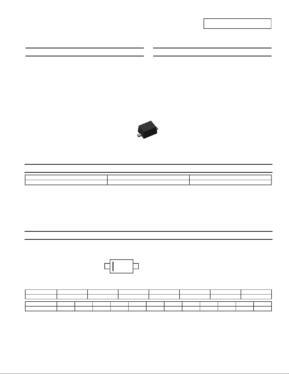
SOD323F
Top View
D3Z2V4BF –D3Z36BF
0.4W SURFACE MOUNT PRECISION ZENER DIODE
Mechanical Data
• Case: SOD323F
• Case Material: Molded Plastic, “Green” Molding Compound.
UL Flammability Classification Rating 94V-0
• Moisture Sensitivity: Level 1 per J-STD-020
• Terminal Connections: Cathode Band
• Terminals: Finish - Matte Tin annealed over Copper Alloy
leadframe. Solderable per MIL-STD-202, Method 208
• Weight: 0.01 grams (approximate)
Ordering Information (Note 4)
Part Number Case Packaging
(Type Number)-7* SOD323F 3000/Tape & Reel
* Example: The part number for the 3.6 Volt device would be D3Z3V6BF-7.
Notes: 1. No purposely added lead. Fully EU Directive 2002/95/EC (RoHS) & 2011/65/EU (RoHS 2) compliant.
2. See http://www.diodes.com for more information about Diodes Incorporated’s definitions of Halogen- and Antimony-free, "Green" and Lead-free.
3. Halogen- and Antimony-free "Green” products are defined as those which contain <900ppm bromine, <900ppm chlorine (<1500ppm total Br + Cl) and
<1000ppm antimony compounds.
4. For packaging details, go to our website at http://www.diodes.com.
Marking Information
Date Code Key
Year 2010 2011 2012 2013 2014 2015 2016
Code X Y Z A B C D
Month Jan Feb Mar Apr May Jun Jul Aug Sep Oct Nov Dec
Code 1 2 3 4 5 6 7 8 9 O N D
XX
YM
D3Z2V4BF – D3Z36BF
Document number: DS35437 Rev. 7 - 2
xx = Product Type Marking Code
(See Electrical Characteristics Table)
YM = Date Code Marking
Y = Year (ex: X = 2010)
M = Month (ex: 9 = September)
1 of 5
www.diodes.com
October 2012
© Diodes Incorporated
Page 2
θ
μ
Maximum Ratings (@T
= +25°C, unless otherwise specified.)
A
Characteristic Symbol Value Unit
Forward Voltage
Thermal Characteristics
Characteristic Symbol Value Unit
Power Dissipation (Note 5)
Thermal Resistance, Junction to Ambient Air (Note 5)
Operating and Storage Temperature Range
NEW PRODUCT NEW PRODUCT
@ I
= 10mA
F
@ IF = 100mA
V
P
R
T
J, TSTG
D3Z2V4BF –D3Z36BF
F
D
JA
0.9
1.1
400 mW
312.5
-65 to +150
V
°C/W
°C
Electrical Characteristics (@T
Zener Voltage Range
Type
Number
Marking
Code
(Note 6)
V
Z @ IZT
Min (V) Max (V) mA
= +25°C, unless otherwise specified.)
A
Maximum Zener Impedance
f = 1kHz
IZT Z
ZT @ IZT
Z
ZK @ IZK
Ω
Maximum Reverse
Current (Note 7)
Temperature
Coefficient
IZK IR @ VR @ IZT = 5mA
mA
A
V mV/°C pF
Typical
Typical Total
Capacitance
= 0V,
@ V
R
f=1MHz
D3Z2V4BF L0 2.43 2.63 5 100 1000 0.5 50 1 -1.6 215
D3Z2V7BF L1 2.69 2.91 5 100 1000 0.5 20 1 -1.7 205
D3Z3V0BF L2 2.85 3.07 5 95 1000 0.5 10 1 -1.7 195
D3Z3V3BF L3 3.32 3.53 5 95 1000 0.5 5 1 -1.9 145
D3Z3V6BF L4 3.60 3.85 5 90 500 1.0 5 1 -2.4 185
D3Z3V9BF L5 3.89 4.16 5 90 500 1.0 3 1 -2.5 175
D3Z4V3BF L6 4.17 4.48 5 90 600 1.0 3 1 -2.5 165
D3Z4V7BF L7 4.55 4.75 5 90 600 1.0 2 1 -1.1 150
D3Z5V1BF GM, L8 4.96 5.20 5 60 250 0.5 2 1.5 0.3 145
D3Z5V6BF L9 5.48 5.73 5 50 100 0.5 1 2.5 1.7 20
D3Z6V2BF LA 6.06 6.33 5 50 80 0.5 0.5 3 2.5 95
D3Z6V8BF LB 6.65 6.93 5 40 60 0.5 0.5 3.5 3.4 82
D3Z7V5BF LC 7.28 7.60 5 10 60 0.5 0.5 4 4.0 70
D3Z8V2BF LD 8.02 8.36 5 10 60 0.5 0.5 5 4.6 57
D3Z9V1BF LE 8.85 9.23 5 10 60 0.5 0.5 6 5.0 50
D3Z10BF LF 9.77 10.21 5 10 60 0.5 0.1 7 6.1 45
D3Z11BF LG 10.78 11.22 5 10 60 0.5 0.1 8 7.4 41
D3Z12BF LH 11.74 12.24 5 10 80 0.5 0.1 9 8.2 36
D3Z13BF LJ 12.91 13.49 5 10 80 0.5 0.1 10 9.4 33
D3Z15BF LK 14.34 14.98 5 15 80 0.5 0.05 11 12.1 28
D3Z16BF LL 15.85 16.51 5 20 80 0.5 0.05 12 13.7 25
D3Z18BF LM 17.56 18.35 5 20 80 0.5 0.05 13 15.8 24
D3Z20BF LN 19.52 20.39 5 20 100 0.5 0.05 15 16.4 22
D3Z22BF LP 21.54 22.47 5 25 100 0.5 0.05 17 18.4 20
D3Z24BF LQ 23.72 24.78 5 30 120 0.5 0.05 19 20.4 18
D3Z27BF LR 26.19 27.53 5 40 150 0.5 0.05 21 18.0 17
D3Z30BF LS 29.19 30.69 5 40 200 0.5 0.05 23 28.6 17
D3Z33BF LT 32.15 33.79 5 40 250 0.5 0.05 25 32.2 15
D3Z36BF LU 35.07 36.87 5 60 300 0.5 0.05 27 34.9 14
Notes: 5. Device mounted on FR-4 PCB with suggested pad layout, board size 35mm * 25mm.
D3Z2V4BF – D3Z36BF
Document number: DS35437 Rev. 7 - 2
6. The Zener voltage is measured 40ms after power is supplied.
7. Short duration pulse test used to minimize self-heating effect.
www.diodes.com
2 of 5
October 2012
© Diodes Incorporated
Page 3

P
P
OWER
PATIO
NSTAN
TANEO
U
O
RWARD CUR
REN
T
NER CUR
REN
T
NER CUR
REN
T
NEW PRODUCT NEW PRODUCT
0.6
Note 5
1,000
(mA)
D3Z2V4BF –D3Z36BF
0.5
N (W)
100
0.4
0.3
DISSI
10
S F
0.2
,
D
1
0.1
F
I, I
0.1
0.4 0.6 0.8 1 1.2 1.4
V , INSTANTANEOUS FORWARD VOLTAGE (V)
F
Fig. 2 Typical Forward Characteristics
20
20
0
250 50 75 100 125 150
T , AMBIENT TEMPERATURE ( C)
A
Fig. 1 Power Derating Curve
°
16
(mA)
12
8
Z
I, ZE
4
0
1345678
2
V , ZENER VOLTAGE (V)
Z
Fig. 3 Typical Zener Breakdown Characteristics
20
15
27BF
30BF
33BF
36BF
10
910
15BF
16BF
18BF
16
12BF
10BF
(mA)
12
8
Z
I, ZE
4
0
8101214161820222426
V , ZENER VOLTAGE (V)
Z
Fig. 4 Typical Zen er B r ea kdown Cha r acteri s t ics
5
Z
I , ZENER CURRENT (mA)
0
28262422
V , ZENER VOLTAGE (V)
30 32 34 36 38 40
Z
Fig. 5 Typical Zener Breakdown Characteristics
D3Z2V4BF – D3Z36BF
Document number: DS35437 Rev. 7 - 2
3 of 5
www.diodes.com
October 2012
© Diodes Incorporated
Page 4

β2β
Package Outline Dimensions
Please see AP02002 at http://www.diodes.com/datasheets/ap02002.pdf for latest version.
NEW PRODUCT NEW PRODUCT
D
α
1
c
α
2
He
E
b (2x)
1
A
L1
Suggested Pad Layout
Please see AP02001 at http://www.diodes.com/datasheets/ap02001.pdf for the latest version.
C
Y (2x)
X (2x)
D3Z2V4BF –D3Z36BF
Dim Min Max Typ
Dimensions Value (in mm)
SOD323F
A 0.60 0.75
b 0.25 0.35
c 0.05 0.26
D 1.15 1.35 1.25
E 1.60 1.80 1.70
He 2.30 2.70 2.50
L1 0.30 0.50 0.40
α1
α2
β1
β2
− −
− −
− −
− −
All Dimensions in mm
X 0.710
Y 0.403
C 2.700
−
−
−
7°
3°
7°
3°
D3Z2V4BF – D3Z36BF
Document number: DS35437 Rev. 7 - 2
4 of 5
www.diodes.com
October 2012
© Diodes Incorporated
Page 5

DIODES INCORPORATED MAKES NO WARRANTY OF ANY KIND, EXPRESS OR IMPLIED, WITH REGARDS TO THIS DOCUMENT,
INCLUDING, BUT NOT LIMITED TO, THE IMPLIED WARRANTIES OF MERCHANTABILITY AND FITNESS FOR A PARTICULAR PURPOSE
(AND THEIR EQUIVALENTS UNDER THE LAWS OF ANY JURISDICTION).
Diodes Incorporated and its subsidiaries reserve the right to make modifications, enhancements, improvements, corrections or other changes
without further notice to this document and any product described herein. Diodes Incorporated does not assume any liability arising out of the
application or use of this document or any product described herein; neither does Diodes Incorporated convey any license under its patent or
trademark rights, nor the rights of others. Any Customer or user of this document or products described herein in such applications shall assume
all risks of such use and will agree to hold Diodes Incorporated and all the companies whose products are represented on Diodes Incorporated
website, harmless against all damages.
Diodes Incorporated does not warrant or accept any liability whatsoever in respect of any products purchased through unauthorized sales channel.
Should Customers purchase or use Diodes Incorporated products for any unintended or unauthorize d application, Customers shall indemnify and
hold Diodes Incorporated and its representatives harmless against all claims, damages, expenses, and attorney fees arising out of, directly or
indirectly, any claim of personal injury or death associated with such unintended or unauthorized application.
Products described herein may be covered by one or more United States, international or foreign patents pending. Product names and markings
noted herein may also be covered by one or more United States, international or foreign trademarks.
NEW PRODUCT NEW PRODUCT
This document is written in English but may be translated into multiple languages for reference. Onl y the English version of this document is the
final and determinative format released by Diodes Incorporated.
Diodes Incorporated products are specifically not authorized for use as critical components in life support devices or systems without the express
written approval of the Chief Executive Officer of Diodes Incorporated. As used herein:
A. Life support devices or systems are devices or systems which:
1. are intended to implant into the body, or
labeling can be reasonably expected to result in significant injury to the user.
B. A critical component is any component in a life support device or system whose failure to perform can be reasonably expected to cause the
failure of the life support device or to affect its safety or effectiveness.
Customers represent that they have all necessary expertise in the safety and regulatory ramifications of their life support devices or systems, and
acknowledge and agree that they are solely responsible for all legal, regulatory and safety-related requirements concerning their products and any
use of Diodes Incorporated products in such safety-critical, life support devices or systems, notwithstanding any devices- or systems-related
information or support that may be provided by Diodes Incorporated. Further, Customers must fully indemnify Diodes Incorporated and its
representatives against any damages arising out of the use of Diodes Incorporated products in such safety-critical, life support devices or systems.
Copyright © 2012, Diodes Incorporated
www.diodes.com
2. support or sustain life and whose failure to perform when properly used in accordance with instructions for use provided in the
IMPORTANT NOTICE
LIFE SUPPORT
D3Z2V4BF –D3Z36BF
D3Z2V4BF – D3Z36BF
Document number: DS35437 Rev. 7 - 2
5 of 5
www.diodes.com
October 2012
© Diodes Incorporated
 Loading...