Diodes D12V0H1U2LP User Manual

)
)
yp
)
Product Summary
V
I
BR (min
12V 13A 80pF
C
PP (max
Description
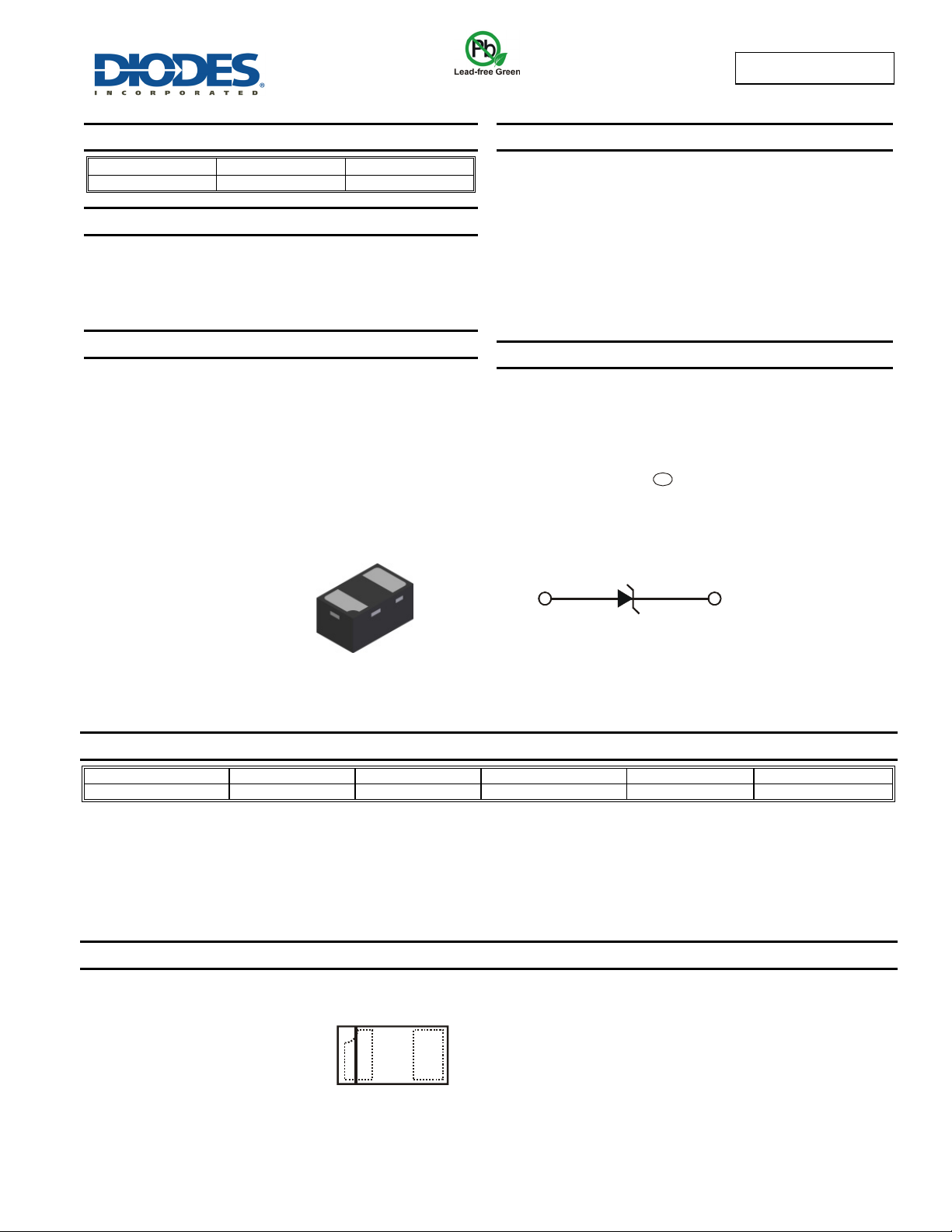
This new generation TVS is designed to protect sensitive electronics
from the damage due to ESD. The combination of small size and high
ESD surge capability makes it ideal for use in portable applications
such as cellular phones, digital cameras, and MP3 players.
Applications
• Cellular Handsets
• Portable Electronics
• Computers and Peripheral
ADVANCE INFORMATION
ADVANCED INFORMATION
X1-DFN1006-2
Bottom View
T(t
D12V0H1U2LP
1 CHANNEL UNIDIRECTIONAL TVS
Features
• Low Profile Package (0.53mm max) and Ultra-small PCB Footprint
Area (1.08 * 0.68mm max) Suitable for Compact Portable
Electronics
• Provides ESD Protection per IEC 61000-4-2 Standard:
Air ±15kV, Contact ±8kV
• 1 Channel of ESD Protection
• Low Channel Input Capacitance
• Totally Lead-Free & Fully RoHS Compliant (Notes 1 & 2)
• Halogen and Antimony Free. “Green” Device (Note 3)
Mechanical Data
• Case: X1-DFN1006-2 with sidewall plating
• Case Material: Molded Plastic, “Green” Molding Compound. UL
Flammability Classification Rating 94V-0
• Moisture Sensitivity: Level 1 per J-STD-020
• Terminals: NiPdAu over Copper leadframe. Solderable per MIL-
STD-202, Method 208
• Weight: 0.001 grams (approximate)
Pin 2 Pin 1
Device Schematic
e4
Ordering Information (Note 4)
Product Compliance Marking Reel Size (inches) Tape Width (mm) Quantity per Reel
D12V0H1U2LP-7B Standard Q2 7 8 10,000/Tape & Reel
Notes: 1. No purposely added lead. Fully EU Directive 2002/95/EC (RoHS) & 2011/65/EU (RoHS 2) compliant.
2. See http://www.diodes.com/quality/lead_free.html for more information about Diodes Incorporated’s definitions of Halogen- and Antimony-free, "Green"
and Lead-free.
3. Halogen- and Antimony-free "Green” products are defined as those which contain <900ppm bromine, <900ppm chlorine (<1500ppm total Br + Cl) and
<1000ppm antimony compounds.
4. For packaging details, go to our website at http://www.diodes.com/products/packages.html.
Marking Information
Q2
D12V0H1U2LP
Document number: DS36751 Rev. 1 - 2
Q2 = Product Type Marking Code
Line Denotes Pin 1 or Cathode Side
1 of 4
www.diodes.com
April 2014
© Diodes Incorporated

P
P
O
R
P
O
N
P
A
P
U
DER
A
TIN
G
O
F
D12V0H1U2LP
Maximum Ratings (@T
= +25°C, unless otherwise specified.)
A
Characteristic Symbol Value Unit Conditions
Peak Pulse Power Dissipation
Peak Pulse Current
ESD Protection – Contact Discharge
ESD Protection – Air Discharge
P
PP
I
PP
V
ESD_Contact
V
ESD_Air
300 W 8/20µs, per Figure 3
13 A 8/20µs, per Figure 3
±30 kV IEC 61000-4-2 Standard
±30 kV IEC 61000-4-2 Standard
Thermal Characteristics
Characteristic Symbol Value Unit
Package Power Dissipation (Note 5)
Thermal Resistance, Junction to Ambient (Note 5)
Operating and Storage Temperature Range
P
D
R
θJA
T
, T
J
STG
ADVANCE INFORMATION
Electrical Characteristics (@T
ADVANCED INFORMATION
Characteristic Symbol Min Typ Max Unit Test Conditions
= +25°C, unless otherwise specified.)
A
Reverse Working Voltage VRWM — — 12.0 V —
Reverse Current (Note 6) IR — 2 50 nA
Reverse Breakdown Voltage VBR 13.3
Reverse Clamping Voltage
Capacitance
Notes: 5. Device mounted on FR-4 PCB pad layout (2oz copper) as shown on Diodes, Inc. suggested pad layout AP02001, which can be found on our website at
http://www.diodes.com.
6. Short duration pulse test used to minimize self-heating effect.
V
CL
C
T
— —
— —
—
250
225
Note 5
200
(mW)
175
—
15.75 V
19
23
80 95 pF
100
75
%
250 mW
500
-65 to +150
V
= V
R
I
= 1mA
R
I
PP
V
I
PP
= 12.0V
RWM
= 5A, tp = 8/20μs
= 13A, tp = 8/20μs
VR = 0V, f = 1MHz
°C/W
°C
ATI
150
125
50
DISSI
100
WE
,
D
75
50
LSE
K
E
25
PEAK POWER OR CURRENT
25
0
0125175
25 10050 75 150
T , AMBIENT TEMPERATURE ( C)
A
°
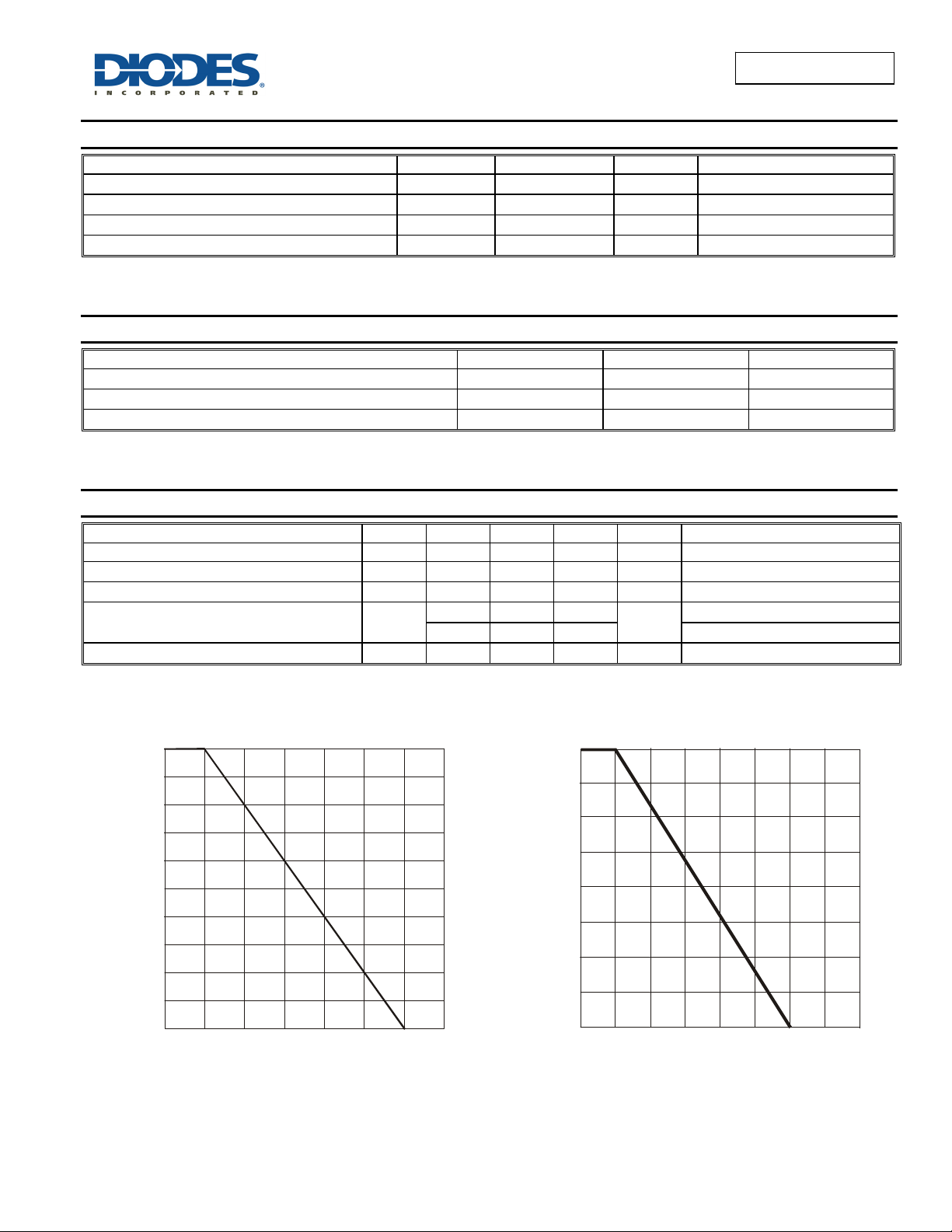
Figure 1 Power Derating Curve
0
0
25 50
T , AMBIENT TEMPERATURE (°C)
A
75 100 125
Figure 2 Pulse Derating Curve
150
175 200
D12V0H1U2LP
Document number: DS36751 Rev. 1 - 2
2 of 4
www.diodes.com
April 2014
© Diodes Incorporated
 Loading...