

Page 1
NEW PRODUCT
Features
• Combines MMBT4401 type transistor with BSS84 type
MOSFET
• Small Surface Mount Package
• PNP/N-Channel Complement Available: CTA2P1N
• Lead Free/RoHS Compliant (Note 2)
• "Green" Device (Note 3 and 4)
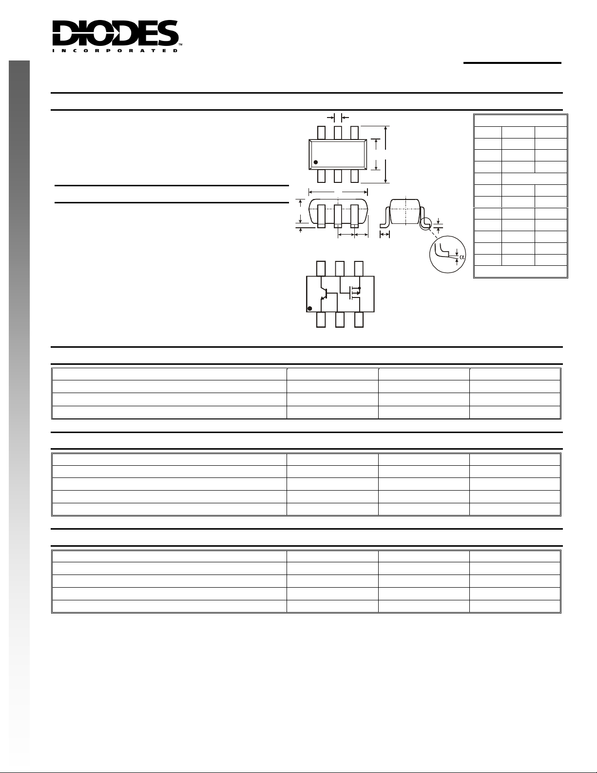
Mechanical Data
• Case: SOT-363
• Case Material: Molded Plastic. UL Flammability
Classification Rating 94V-0
• Moisture Sensitivity: Level 1 per J-STD-020C
• Terminals: Solderable per MIL-STD-202, Method 208
• Lead Free Plating (Matte Tin Finish annealed over Alloy 42
leadframe).
• Terminal Connections: See Diagram
• Marking Information: A03, See Page 6
• Ordering Information: See Page 6
• Weight: 0.006 grams (approximate)
CTA2N1P
COMPLEX TRANSISTOR ARRAY
A
A03
H
K
J
Q1
CQ1G
E
Q1
D
Q2
B
Q1
SOT-363
Dim Min Max
A 0.10 0.30
C
B
B 1.15 1.35
C 2.00 2.20
D 0.65 Nominal
F 0.30 0.40
H 1.80 2.20
M
J
⎯
0.10
K 0.90 1.00
L
F
S
Q2
Q2
D
Q2
L 0.25 0.40
M 0.10 0.25
α
All Dimensions in mm
0°
8°
Maximum Ratings, Total Device @T
= 25°C unless otherwise specified
A
Characteristic Symbol Value Unit
Power Dissipation (Note 1)
Thermal Resistance, Junction to Ambient (Note 1)
Operating and Storage Temperature Range
R
Tj, T
Pd
θ
JA
STG
Maximum Ratings, Q1, MMBT4401 NPN Transistor Element @T
150 mW
833
-55 to +150
= 25°C unless otherwise specified
A
Characteristic Symbol Value Unit
Collector-Base Voltage
Collector-Emitter Voltage
Emitter-Base Voltage
Collector Current - Continuous
V
V
V
CBO
CEO
EBO
IC
Maximum Ratings, Q2, BSS84 P-Channel MOSFET Element @T
60 V
40 V
6.0 V
600 mA
= 25°C unless otherwise specified
A
Characteristic Symbol Value Unit
Drain-Source Voltage
Drain-Gate Voltage R
≤ 1.0MΩ V
GS
Gate-Source Voltage Continuous
Drain Current Continuous
Notes: 1. Device mounted on FR-4 PCB, 1 inch x 0.85 inch x 0.062 inch; pad layout as shown on Diodes Inc. suggested pad layout
Code UO are built with Non-Green Molding Compound and may contain Halogens or Sb2O3 Fire Retardants.
document AP02001, which can be found on our website at http://www.diodes.com/datasheets/ap02001.pdf.
2. No purposefully added lead.
3. Diodes Inc.'s "Green" policy can be found on our website at http://www.diodes.com/products/lead_free/index.php.
4. Product manufactured with Date Code UO (week 40, 2007) and newer are built with Green Molding Compound. Product manufactured prior to Date
V
V
DSS
DGR
GSS
ID
-50 V
-50 V
±20 V
-130 mA
DS30295 Rev. 7 - 2 1 of 6
www.diodes.com
°C/W
°C
CTA2N1P
© Diodes Incorporated
Page 2
NEW PRODUCT
Electrical Characteristics, Q1, MMBT4401 NPN Transistor Element @T
Characteristic Symbol Min Max Unit Test Condition
OFF CHARACTERISTICS (Note 5)
Collector-Base Breakdown Voltage
Collector-Emitter Breakdown Voltage
Emitter-Base Breakdown Voltage
Collector Cutoff Current
Base Cutoff Current
ON CHARACTERISTICS (Note 5)
DC Current Gain
Collector-Emitter Saturation Voltage
Base-Emitter Saturation Voltage
SMALL SIGNAL CHARACTERISTICS
Output Capacitance
Input Capacitance
Input Impedance
Voltage Feedback Ratio
Small Signal Current Gain
Output Admittance
Current Gain-Bandwidth Product
SWITCHING CHARACTERISTICS
Delay Time
Rise Time
Storage Time
Fall Time
V
(BR)CBO
V
(BR)CEO
V
(BR)EBO
I
CEX
IBL
hFE
V
CE(SAT)
V
BE(SAT)
Ccb
Ceb
hie
hre
hfe
hoe
fT
td
tr
ts
tf
60
40
6.0
⎯
⎯
20
40
80
100
40
⎯
0.75
0.40
0.75
0.95
⎯
⎯
⎯
1.0 15
0.1 8.0 x 10⁻⁴
40 500
1.0 30
250
⎯
⎯
⎯
⎯
⎯
⎯
⎯
V
V
V
100 nA
100 nA
⎯
⎯
⎯
⎯
300
⎯
V
1.2
V
6.5 pF
30 pF
kΩ
⎯
μS
⎯
MHz
15 ns
20 ns
225 ns
30 ns
= 25°C unless otherwise specified
A
IC = 100μA, IE = 0
IC = 1.0mA, IB = 0
IE = 100μA, IC = 0
V
= 35V, V
CE
V
= 35V, V
CE
IC = 100µA, V
EB(OFF)
EB(OFF)
= 1.0V
CE
= 0.4V
= 0.4V
IC = 1.0mA, VCE = 1.0V
IC = 10mA, VCE = 1.0V
IC = 150mA, V
CE
= 1.0V
IC = 500mA, VCE = 2.0V
IC = 150mA, IB = 15mA
IC = 500mA, IB = 50mA
IC = 150mA, IB = 15mA
IC = 500mA, IB = 50mA
VCB = 5.0V, f = 1.0MHz, IE = 0
VEB = 0.5V, f = 1.0MHz, IC = 0
V
= 10V, IC = 1.0mA,
CE
f = 1.0kHz
VCE = 10V, IC = 20mA,
f = 100MHz
VCC = 30V, IC = 150mA,
V
= 2.0V, IB1 = 15mA
BE(off)
VCC = 30V, IC = 150mA,
IB1 = IB2 = 15mA
Electrical Characteristics, Q2, BSS84 P-Channel MOSFET Element @T
Characteristic Symbol Min Typ Max Unit Test Condition
OFF CHARACTERISTICS (Note 5)
Drain-Source Breakdown Voltage
Zero Gate Voltage Drain Current
Gate-Body Leakage
BV
I
I
GSS
DSS
DSS
-50
⎯
⎯
⎯
⎯ ⎯
⎯ ⎯
⎯
-15
-60
⎯
-100
⎯
±10
V
µA
µA
nA
nA
ON CHARACTERISTICS (Note 5)
Gate Threshold Voltage
Static Drain-Source On-Resistance
Forward Transconductance
V
GS(th)
R
DS (ON)
gFS
-0.8
⎯ ⎯
.05
-2.0 V
⎯
10
⎯ ⎯
Ω
S
DYNAMIC CHARACTERISTICS
Input Capacitance
Output Capacitance
Reverse Transfer Capacitance
C
C
oss
C
⎯ ⎯
iss
⎯ ⎯
⎯ ⎯
rss
45 pF
25 pF
12 pF
SWITCHING CHARACTERISTICS
Turn-On Delay Time
Turn-Off Delay Time
Notes: 5. Short duration pulse test used to minimize self-heating effect.
t
D(ON)
t
D(OFF)
⎯
⎯
10
18
⎯
⎯
ns
ns
DS30295 Rev. 7 - 2 2 of 6
www.diodes.com
= 25°C unless otherwise specified
A
VGS = 0V, ID = -250µA
V
= -50V, VGS = 0V, TJ = 25°C
DS
V
= -50V, VGS = 0V, TJ = 125°C
DS
V
= -25V, VGS = 0V, TJ = 25°C
DS
VGS = ±20V, V
DS
= 0V
VDS = VGS, ID = -1mA
VGS = -5V, ID = 0.100A
V
= -25V, ID = 0.1A
DS
VDS = -25V, V
GS
= 0V
f = 1.0MHz
V
= -30V, ID = -0.27A,
DD
R
= 50Ω, V
GEN
GS
= -10V
CTA2N1P
© Diodes Incorporated
Page 3

P, P
OWER
P
TIO
C CUR
R
N
T
GAIN
NEW PRODUCT
CAPACITANC
F
C
O
CTO
R
T
TER VOLTAG
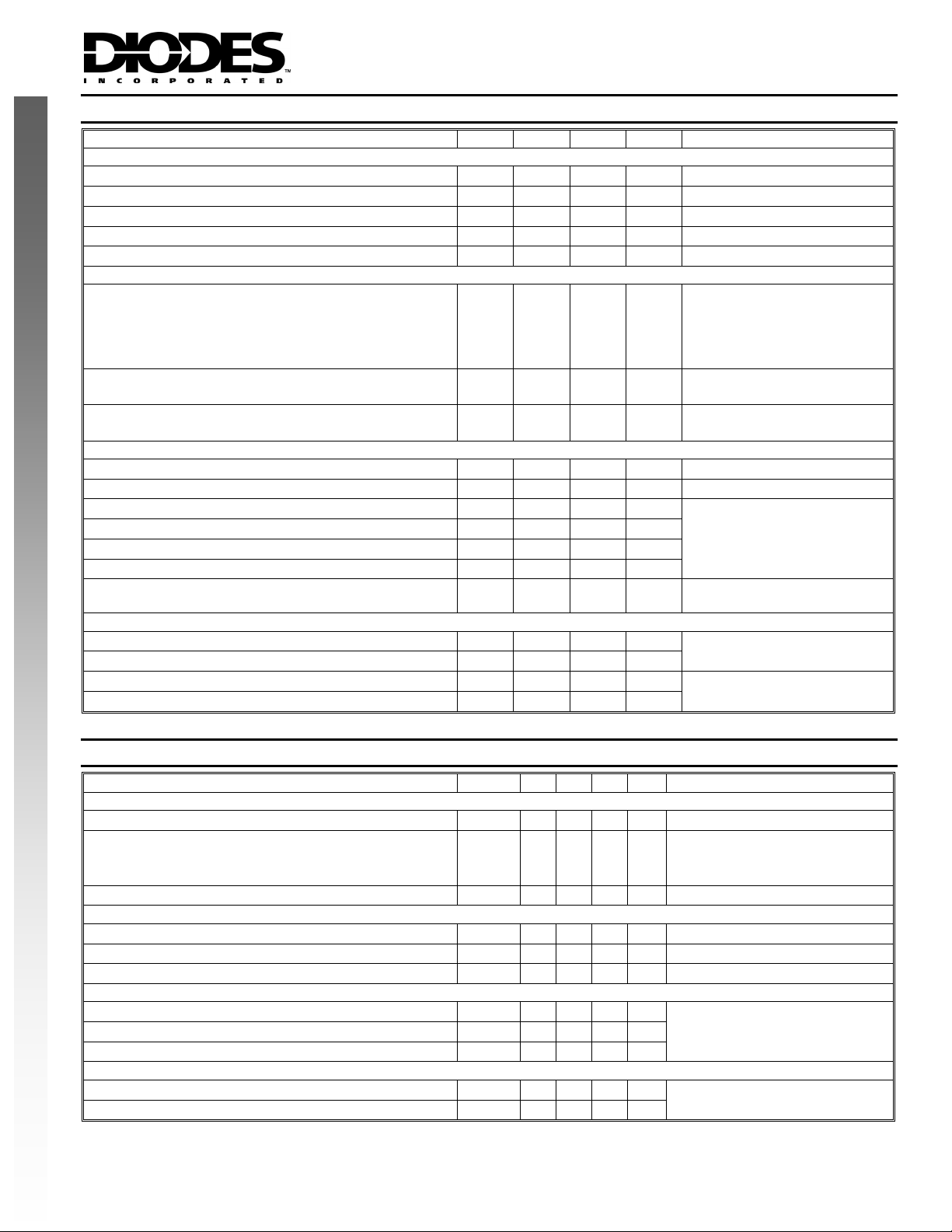
MMBT4401 Section
N (mW)
A
DISSI
D
200
150
100
50
0
0
25 50
T , AMBIENT TEMPERATURE (°C)
A
75 100 125
150
175
200
Fig. 1 Max Power Dissipation vs.
Ambien t Temper at ur e (Total Device)
1,000
T = 125°C
A
100
E
FE
h, D
10
T = -25°C
A
1
0.1
T = +25°C
A
1
I , COLLECTOR CURRENT (mA)
C
10 1,000
Fig. 2 Typical DC Current Gain vs. Collector Current
V = 1.0V
100
CE
30
20
C
ibo
)
10
E (p
E (V)
-EMI
2.0
1.8
1.6
1.4
1.2
1.0
I = 1mA
C
I = 10mA
C
I = 30mA
C
I = 100mA
C
I = 300mA
C
0.8
5.0
C
obo
1.0
0.1
101.0 50
REVERSE VOLTAGE (V)
Fig. 3 Typical Capacitance
LLE
V,
CE
0.6
0.4
0.2
0
0.001
0.01 1 10
0.1 100
I , BASE CURRENT (mA)
B
Fig. 4 Typical Collector Saturation Region
DS30295 Rev. 7 - 2 3 of 6
www.diodes.com
CTA2N1P
© Diodes Incorporated
Page 4

T
TER VOLTAG
C
O
CTO
R
T
O
MIT
TER
NEW PRODUCT
GAIN
N
DWIDTH PRODUCT (M
H
MMBT4401 Section
E (V)
BE(ON)
V , BASE EMI
1.0
V = 5V
0.9
0.8
0.7
CE
T = -50°C
A
T = 25°C
A
0.6
0.5
T = 150°C
A
0.4
0.3
0.2
10.1 10 100
I , COLLECTOR CURRENT (mA)
C
Fig. 6 Base Emitter Voltage vs. Collector Current
E
LLE
SATURATION VOLTAGE (V)
CE(SAT)
V,
0.5
I
C
= 10
I
B
0.4
0.3
T = 150°C
A
0.2
0.1
0
110
I , COLLECTOR CURRENT (mA)
C
Fig. 5 Collector Emitter Saturation Vo ltage
vs. Collector Current
T = 25°C
A
100
T = -50°C
A
1,000
1,000
z)
100
10
BA
T
f,
1
110
I , COLLECTOR CURRENT (mA)
C
Fig. 7 Gain Ba ndwidth Product vs. C ol l ect or Current
100
DS30295 Rev. 7 - 2 4 of 6
www.diodes.com
CTA2N1P
© Diodes Incorporated
Page 5

R
N-T
O-SOUR
CE CUR
REN
T
R
CUR
RENT
BSS84 Section
600
500
(mA)
-1.0
-0.8
NEW PRODUCT
400
(A)
-0.6
300
-0.4
AIN
200
D
AI
100
D
I, D
0
0215
V , DRAIN-TO-SOURCE VOLTAGE (V)
DS
3
4
I, D
-0.2
-0.0
Fig. 8 Drain-Source Current vs.
Drain-Source Voltage
10
15
9
8
12
Ω
7
6
5
4
0-2-3-4-1
V , GATE-TO-SOURCE VOLTAGE (V)
GS
-5
Fig. 9 Drain Current vs. Gate Source Voltage
V = -10V
GS
I = -0.13A
D
9
6
-6
-8-7
3
DS(ON)
R , ON-RESISTA N CE ( )
2
1
T = 25C
°
0
0
1234
V , GATE-TO-SOURCE VOLTAGE (V)
GS
A
Fig. 10 On- R esistance vs. Gate-S our ce Voltage
25.0
T = 125C
°
A
5
3
0
-50
-25
T , JUNCTION TEMPERATURE (°C)
J
25
0
75 150
50 125
100
Fig. 11 On-Resistance vs. Junction Temperature
20.0
V = -3.5V
V = -3V
GS
15.0
10.0
V = -4V
5.0
0.0
-0.0
-0.2
I , DRAIN CURRENT (A)
D
Fig. 12, On-Resistance vs. Drain Current
DS30295 Rev. 7 - 2 5 of 6
GS
V = -4.5V
GS
GS
-0.4 -0.6
V = -5V
GS
V = -6V
GS
V = -8V
GS
V = -10V
GS
-0.8
1.0
www.diodes.com
CTA2N1P
© Diodes Incorporated
Page 6

A
A
Ordering Information (Note 6)
NEW PRODUCT
Device
CTA2N1P-7-F
Notes: 6. For packaging details, go to our website at http://www.diodes.com/datasheets/ap02007.pdf.
Packaging Shipping
SOT-363 3000/Tape & Reel
Marking Information
Date Code Key
Year 2001 2002 2003 2004 2005 2006 2007 2008 2009 2010 2011 2012
Code M N P R S T U V W X Y Z
Month Jan Feb Mar Apr May Jun Jul Aug Sep Oct Nov Dec
Code 1 2 3 4 5 6 7 8 9 O N D
Diodes Incorporated and its subsidiaries reserve the right to make modifications, enhancements, improvements, corrections or other changes
without further notice to any product herein. Diodes Incorporated does not assume any liability arising out of the application or use of any product
described herein; neither does it convey any license under its patent rights, nor the rights of others. The user of products in such applications shall
assume all risks of such use and will agree to hold Diodes Incorporated and all the companies whose products are represented on our website,
harmless against all damages.
Diodes Incorporated products are not authorized for use as critical components in life support devices or systems without the expressed written
approval of the President of Diodes Incorporated.
03
03 = Product Type Marking Code
YM = Date Code Marking
Y = Year ex: T = 2006
YM
M = Month ex: 9 = September
IMPORTANT NOTICE
LIFE SUPPORT
DS30295 Rev. 7 - 2 6 of 6
www.diodes.com
CTA2N1P
© Diodes Incorporated
 Loading...