Diodes BAW101 User Manual

BAW101
DUAL SURFACE MOUNT SWITCHING DIODE
Features
• Fast Switching Speed
• High Reverse Breakdown Voltage
• Two Electrically Isolated Elements in a Single Compact Package
• Low Leakage Current
• Lead, Halogen and Antimony Free, RoHS Compliant (Note 1)
• "Green" Device (Note 2)
NEW PRODUCT
Mechanical Data
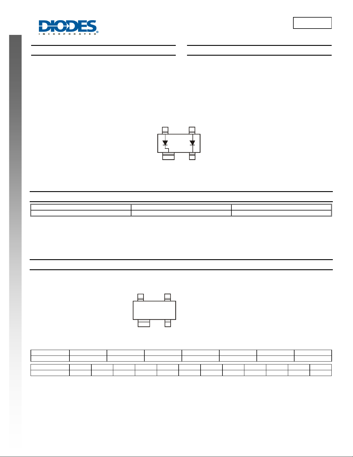
• Case: SOT143
• Case Material: Molded Plastic. UL Flammability Classification
Rating 94V-0
• Moisture Sensitivity: Level 1 per J-STD-020
• Lead Free Plating (Matte Tin Finish annealed over Alloy 42
leadframe).
• Polarity: See Diagram Below
• Weight: 0.008 grams (approximate)
Device Schematic
Ordering Information (Note 3)
Part Number Case Packaging
BAW101-7 SOT143 3000/Tape & Reel
Notes: 1. No purposefully added lead. Halogen and Antimony free.
2. Diodes Inc.`s “Green” Policy can be found on our website at http://www.diodes.com
3. For packaging details, go to our website at http://www.diodes.com.
Marking Information
Date Code Key
Year 2011 2012 2013 2014 2015 2016 2017
Code Y Z A B C D E
Month Jan Feb Mar Apr May Jun Jul Aug Sep Oct Nov Dec
Code 1 2 3 4 5 6 7 8 9 O N D
BAW101
Document number: DS32092 Rev. 3 - 2
KT9
www.diodes.com
KT9 = Product Type Marking Code
YM = Date Code Marking
Y = Year (ex: Y = 2011)
YM
M = Month (ex: 9 = September)
1 of 4
June 2011
© Diodes Incorporated

)
θ
(BR)
P, P
O
R
P
T
O
Maximum Ratings @T
= 25°C unless otherwise specified
A
Characteristic Symbol Value Unit
Repetitive Peak Reverse Voltage
Series Connection
Working Peak Reverse Voltage
DC Blocking Voltage
Series Connection
RMS Reverse Voltage
Forward Current (Note 4)
Single Diode Loaded
Double Diode Loaded
Non-Repetitive Peak Forward Surge Current Square Wave @ t = 1.0μs
Repetitive Peak Forward Current (Note 4)
NEW PRODUCT
Thermal Characteristics
Characteristic Symbol Value Unit
Power Dissipation (Note 4)
Thermal Resistance Junction to Ambient Air (Note 4)
Operating and Storage Temperature Range
Single Diode
Single Diode
BAW101
V
RRM
V
RWM
V
R
V
R(RMS
I
F
I
FSM
I
FRM
P
D
R
JA
, T
T
J
STG
300
600
300
600
212 V
250
140
4.5 A
625 mA
400 mW
312
-65 to +150
V
V
mA
°C/W
°C
Electrical Characteristics @T
= 25°C unless otherwise specified
A
Characteristic Symbol Min Max Unit Test Condition
Reverse Breakdown Voltage (Note 5)
Forward Voltage
Reverse Current (Note 5)
Total Capacitance
Reverse Recovery Time
Notes: 4. Part mounted on FR-4 board with recommended pad layout, which can be found on our website at http://www.diodes.com.
5. Short duration pulse test used to minimize self-heating effect.
V
R
V
F
I
R
C
⎯
T
t
⎯
rr
300
⎯
⎯
⎯
⎯
1.1 V
150
75
2.0 pF
50 ns
V
nA
μA
500
Note 4
1,000
400
N (mW)
I
A
300
100
T = 150ºC
T = 125ºC
A
A
DISSI
200
WE
D
100
10
IR = 100μA
IF = 100mA
= 250V
V
R
V
= 250V, TJ = 150°C
R
VR = 0, f = 1.0MHz
= IR = 30mA,
I
F
I
= 0.1 x IR, RL = 100Ω
rr
T = 85ºC
A
T = 25ºC
A
T = -55ºC
A
0
0
25
T , AMBIENT TEMPERATURE ( C)
A
50
75
100
125
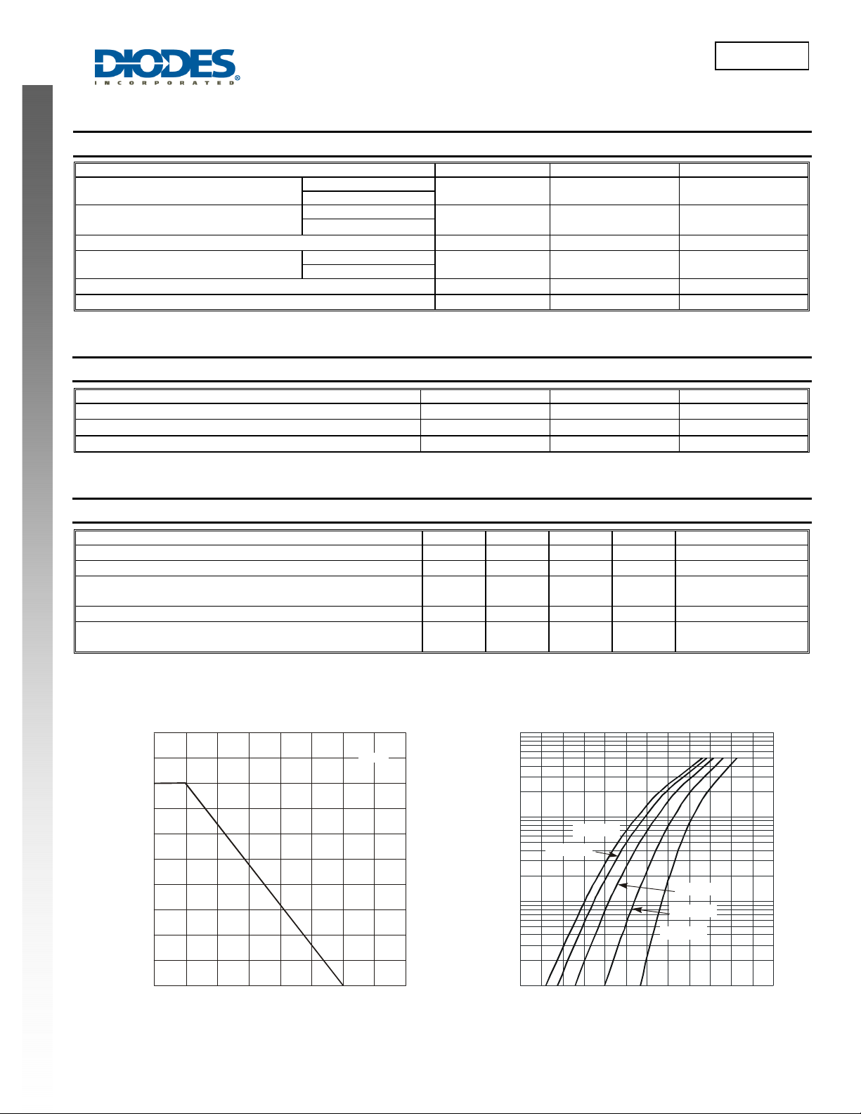
Fig. 1 Power Derating Curve, To ta l Package
150 200
175
°
1
F
I , INSTANTANEOUS FORWARD CURRENT (mA)
0.40.2
V , INSTANTANEOUS FORWARD VOL TAGE (V)
F
0.6
0.8
1.0
Fig. 2 Typical Forward Characteristics, Per Element
1.2
1.4
BAW101
Document number: DS32092 Rev. 3 - 2
2 of 4
www.diodes.com
June 2011
© Diodes Incorporated
 Loading...