BAT54TW /ADW /CDW /SDW /BRW
Document number: DS30152 Rev. 17 - 2
1 of 4
www.diodes.com
June 2016
© Diodes Incorporated
BAT54TW /ADW / CDW /SDW /BRW
Features
Low Forward Voltage Drop
Fast Switching
Ultra-Small Surface Mount Package
PN Junction Guard Ring for Transient and ESD Protection
Totally Lead-Free & Fully RoHS Compliant (Notes 1 & 2)
Halogen and Antimony Free.“Green”Devise (Note 3)
Mechanical Data
Case: SOT-363
Case Material: Molded Plastic.
UL Flammability Classification Rating 94V-0
Moisture Sensitivity: Level 1 per J-STD-020D
Terminals: Solderable per MIL-STD-202, Method 208
Lead Free Plating (Matte Tin Finish annealed over Alloy 42
Leadframe).
Weight: 0.006 grams (Approximate)
A
1
A
2
C
2
C
1
C
2
C
1
C
1
C
2
A
2
A
1
A
2
A
1
AC
1
AC
2
C
2
A
1
A
2
C
1
AC
1
AC
2
C
1
A
1
C
2
A
2
C
1
A
3
C
2
A
1
C
3
A
2
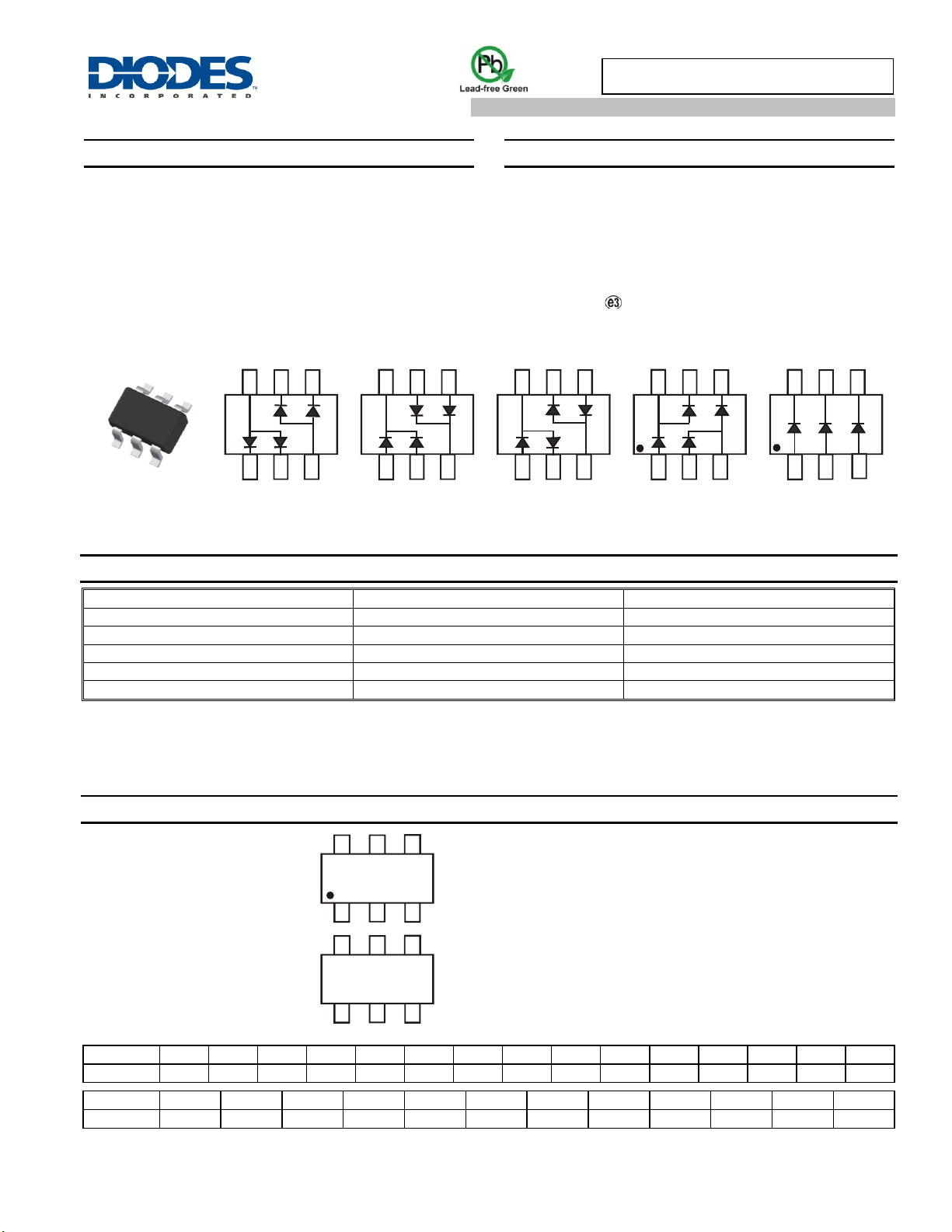
Top View
BAT54ADW*
BAT54CDW*
BAT54SDW*
BAT54BRW
BAT54TW
Part Number
Case
Packaging
BAT54ADW-7-F
SOT-363
3,000/Tape & Reel
BAT54CDW-7-F
SOT-363
3,000/Tape & Reel
BAT54SDW-7-F
SOT-363
3,000/Tape & Reel
BAT54BRW-7-F
SOT-363
3,000/Tape & Reel
BAT54TW-7-F
SOT-363
3,000/Tape & Reel
Year
2001
2002 … 2011
2012
2013
2014
2015
2016
2017
2018
2019
2020
2021
2022
Code
M N … Y Z A B C D E F G H I J
Month
Jan
Feb
Mar
Apr
May
Jun
Jul
Aug
Sep
Oct
Nov
Dec
Code
1 2 3 4 5 6 7 8 9 O N
D
Kxx = Product Type Marking Code
For Symmetrical Configuration, No Orientation Indicator
KL6 = BAT54ADW
KL7 = BAT54CDW
KL8 = BAT54SDW
KLB = BAT54BRW
KLA = BAT54TW
YM = Date Code Marking
Y = Year (ex: D = 2016)
M = Month (ex: 9 = September)
Kxx
YM
Kxx YM
Kxx YM
SURFACE MOUNT SCHOTTKY BARRIER DIODE ARRAYS
*Symmetrical configuration, no orientation indicator.
Ordering Information (Note 4)
Notes: 1. No purposely added lead. Fully EU Directive 2002/95/EC (RoHS) & 2011/65/EU (RoHS 2) compliant.
2. See http://www.diodes.com/quality/lead_free.html for more information about Diodes Incorporated’s definitions of Halogen- and Antimony-free, "Green"
and Lead-free.
3. Halogen- and Antimony-free "Green” products are defined as those which contain <900ppm bromine, <900ppm chlorine (<1500ppm total Br + Cl) and
<1000ppm antimony compounds.
4. For packaging details, go to our website at http://www.diodes.com/products/packages.html.
Marking Information
Date Code Key

BAT54TW /ADW /CDW /SDW /BRW
Document number: DS30152 Rev. 17 - 2
2 of 4
www.diodes.com
June 2016
© Diodes Incorporated
BAT54TW /ADW / CDW /SDW /BRW
Characteristic
Symbol
Value
Unit
Peak Repetitive Reverse Voltage
Working Peak Reverse Voltage
DC Blocking Voltage
V
RRM
V
RWM
VR
30
V
Forward Continuous Current (Note 5)
IF
200
mA
Repetitive Peak Forward Current (Note 5)
I
FRM
300
mA
Forward Surge Current (Note 5) @ t < 1.0s
I
FSM
600
mA
Characteristic
Symbol
Value
Unit
Power Dissipation (Note 5)
PD
200
mW
Thermal Resistance, Junction to Ambient Air (Note 5)
R
JA
625
°C/W
Operating and Storage Temperature Range
TJ, T
STG
-65 to +125
°C
Characteristic
Symbol
Min
Typ
Max
Unit
Test Condition
Reverse Breakdown Voltage (Note 6)
V
(BR)R
30
V
IR = 100µA
Forward Voltage (Note 6)
VF
240
320
400
500
1,000
mV
IF = 0.1mA
IF = 1mA
IF = 10mA
IF = 30mA
IF = 100mA
Reverse Leakage Current (Note 6)
IR
2.0
µA
VR = 25V
Total Capacitance
CT
10
pF
VR = 1.0V, f = 1.0MHz
Reverse Recovery Time
trr
5.0
ns
IF = 10mA through IR = 10mA
to IR = 1.0mA, RL = 100Ω
0.1
0.01
1
0.001
0.0001
0
1.00.4
0.6
0.8
0.2
I , INSTANTANEOUS FORWARD CURRENT (A)
F
V , INSTANTANEOUS FORWARD VOLTAGE (V)
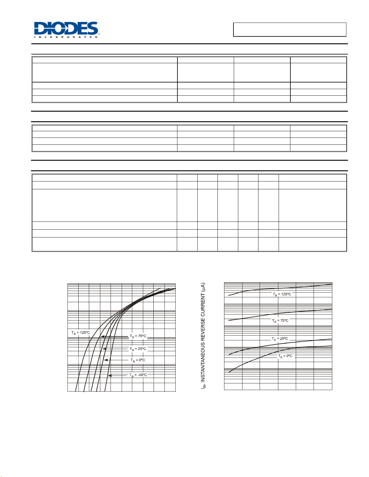
Fig. 1 Typical Forward Characteristics
F
0.001
0.01
0.1
10
1
100
0
5 10 15 20
25
30
V , INSTANTANEOUS REVERSE VOLTAGE (V)
Fig. 2 Typical Reverse Characteristics
R
Maximum Ratings (@T
= +25°C, unless otherwise specified.)
A
Thermal Characteristics
Electrical Characteristics (@T
= +25°C, unless otherwise specified.)
A
Notes: 5. Device mounted on FR-4 PCB, 1 inch x 0.85 inch x 0.062 inch; pad layout, which can be found on our website at
http://www.diodes.com/package-outlines.html.
6. Short duration pulse test used to minimize self-heating effect.
 Loading...