Features
• Guard Ring Die Construction for Transient Protection
• Low Power Loss, High Efficiency
• Surge Overload Rating to 100A Peak
• For Use in Low Voltage, High Frequency Inverters, Free
Wheeling, and Polarity Protection Application
• Lead Free Finish/RoHS Compliant (Note 1)
• Green Molding Compound (No Halogen and Antimony)
(Note 2)
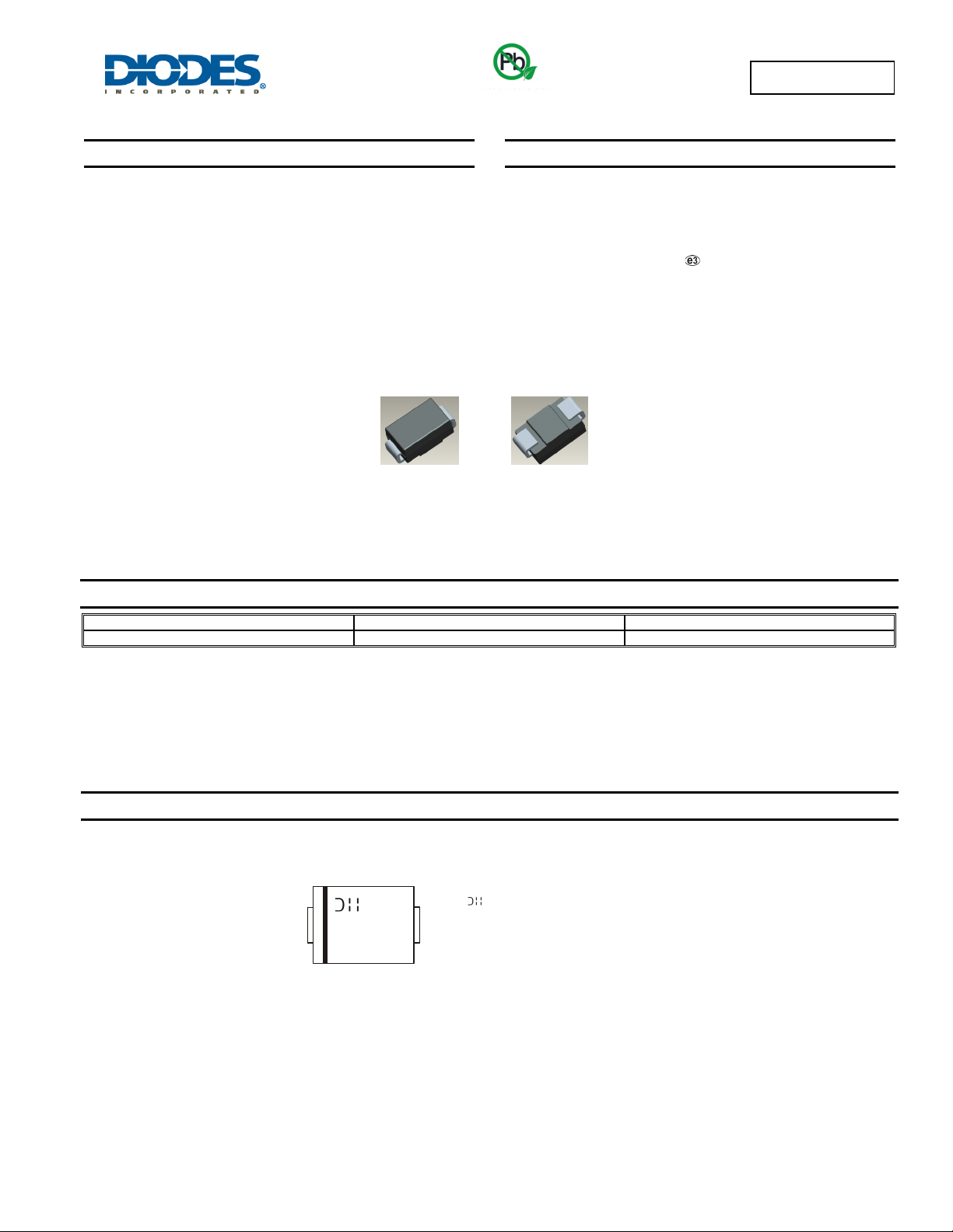
Top View
Green
B370 - B3100
3.0A HIGH VOLTAGE SCHOTTKY BARRIER RECTIFIER
Mechanical Data
• Case: SMC
• Case Material: Molded Plastic. UL Flammability Classification
Rating 94V-0
• Moisture Sensitivity: Level 1 per J-STD-020
• Terminals: Lead Free Plating (Matte Tin Finish). Solderable per
MIL-STD-202, Method 208
• Polarity: Cathode Band or Cathode Notch
• Weight: 0.21 grams (approximate)
Bottom View
Ordering Information (Note 3)
Part Number* Case Packaging
B3x0-13-F SMC 3000/Tape & Reel
* x = Device type, e.g. B380-13-F (SMC package).
Notes: 1. EU Directive 2002/95/EC (RoHS). All applicable RoHS exemptions applied, see EU Directive 2002/95/EC Annex Notes.
2. Product manufactured with Data Code 0924 (week 24, 2009) and newer are built with Green Molding Compound.
3. For packaging details, go to our website at http://www.diodes.com.
Marking Information
B370 - B3100
Document number: DS30020 Rev. 14 - 2
B3x0
YWW
B3x0 = Product type marking code, ex: B380 (SMC package)
= Manufacturers’ code marking
YWW = Date code marking
Y = Last digit of year (ex: 2 for 2002)
WW = Week code (01 - 53)
Note: B3100 marking code is B3100
1 of 4
www.diodes.com
March 2011
© Diodes Incorporated

)
θ
NST
N
T
N
O
US F
O
RWARD C
URR
N
T
C, TOT
CAPACITANC
F
Maximum Ratings @T
= 25°C unless otherwise specified
A
Single phase, half wave, 60Hz, resistive or inductive load.
For capacitance load, derate current by 20%.
Characteristic Symbol B370 B380 B390 B3100 Unit
Peak Repetitive Reverse Voltage
Working Peak Reverse Voltage
V
V
DC Blocking Voltage (Note 4)
RMS Reverse Voltage
V
R(RMS
Average Rectified Output Current @ TT = 90°C IO
Non-Repetitive Peak Forward Surge Current 8.3ms
single half sine-wave superimposed on rated load
Notes: 4. VB measured at IR = 500μA (25°C).
I
Thermal Characteristics
Characteristic Symbol Value Unit
Typical Thermal Resistance Junction to Terminal
Operating Temperature Range
Storage Temperature Range
RRM
RWM
VR
FSM
B370 - B3100
70 80 90 100 V
49 56 63 70 V
3.0 A
R
JT
T
J
T
STG
100 A
10
-55 to +125
-55 to +150
°C/W
°C
°C
Electrical Characteristics @T
= 25°C unless otherwise specified
A
Characteristic Symbol Min Typ Max Unit Test Condition
= 3.0A, TA = 25°C
Forward Voltage Drop
Leakage Current (Note 5)
Total Capacitance
Notes: 5. Short duration pulse test used to minimize self-heating effect.
10
V
F
I
R
C
T
-
-
-
-
- - 100 pF
0.79
-
-
0.69
-
-
0.5
20
1,000
I
F
V
= 3.0A, TA = 100°C
I
F
@ Rated V
mA
@ Rated V
VR = 4V, f = 1MHz
, TA = 25°C
R
, TA = 100°C
R
(A)
E
)
E (p
1.0
100
AL
0.1
E
A
T
A
T = 25°C
J
I Pulse Width = 300µs
F
I, I
0.01
0 0.2 0.4 0.6 0.8 1.0
V , INSTANTANEOUS FORWARD VOL TAGE (V)
F
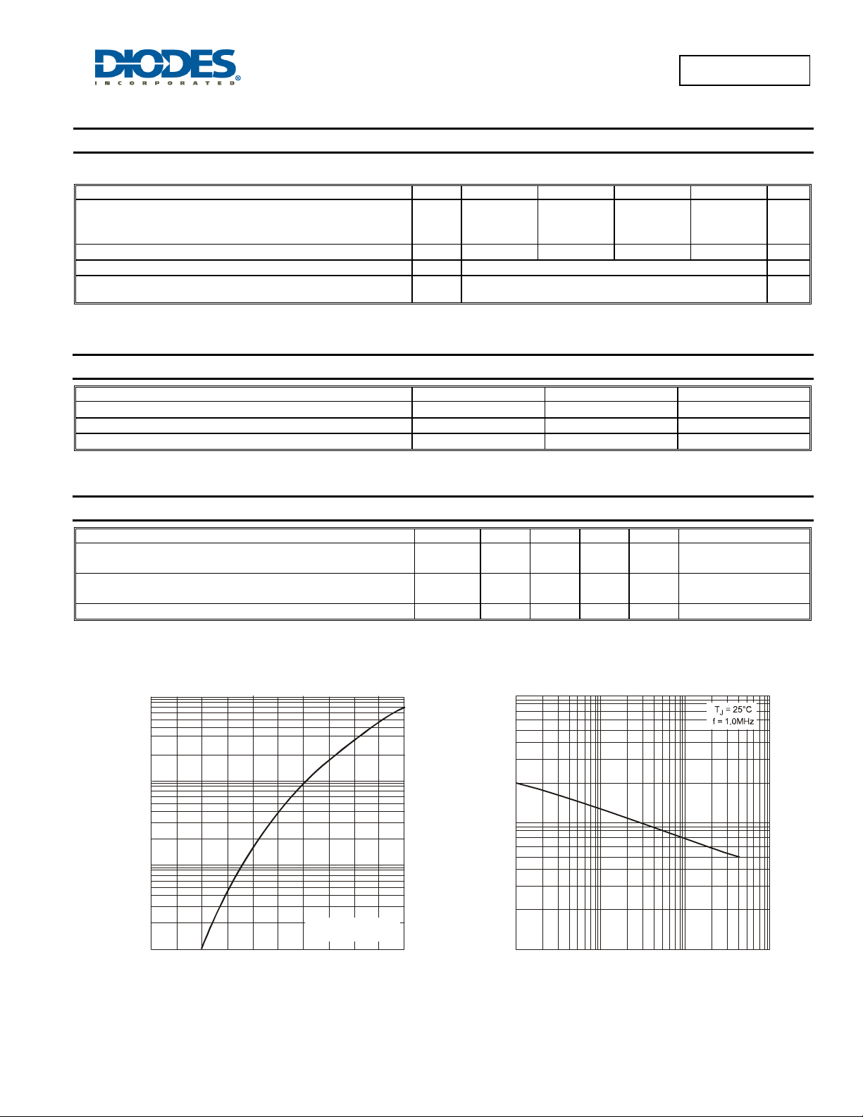
Fig. 1 Typical Forward Characteristics
F
10
0.1 1 10 100
V , DC REVERSE VOLTAGE (V)
R
Fig. 2 Total Capacitance vs. Reverse Voltage
B370 - B3100
Document number: DS30020 Rev. 14 - 2
2 of 4
www.diodes.com
March 2011
© Diodes Incorporated
 Loading...