

Page 1
Features
• Guard Ring Die Construction for Transient Protection
• Ideally Suited for Automated Assembly
• Low Power Loss, High Efficiency
• Surge Overload Rating to 50A Peak
• For Use in Low Voltage, High Frequency Inverters, Free
Wheeling, and Polarity Protection Application
• High Temperature Soldering: 260°C/10 Second at Terminal
• Lead Free Finish, RoHS Compliant (Note 1)
• Green Molding Compound (No Halogen and Antimony)
(Note 2)
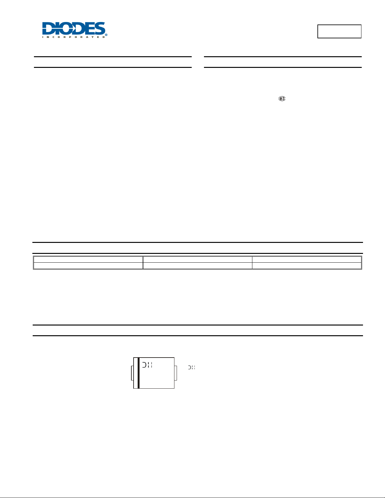
Top View
Green
B1100LB
1.0A HIGH VOLTAGE SCHOTTKY BARRIER RECTIFIER
Mechanical Data
• Case: SMB
• Case Material: Molded Plastic. UL Flammability Classification
Rating 94V-0
• Terminals: Lead Free Plating (Matte Tin Finish). Solderable per
MIL-STD-202, Method 208
• Polarity: Cathode Band or Cathode Notch
• Weight: 0.093 grams (approximate)
Bottom View
Ordering Information (Note 3)
Part Number Case Packaging
B1100LB-13-F SMB 3000/Tape & Reel
Notes: 1. EU Directive 2002/95/EC (RoHS). All applicable RoHS exemptions applied, see EU Directive 2002/95/EC Annex Notes.
2. Product manufactured with Data Code 0924 (week 24, 2009) and newer are built with Green Molding Compound.
3. For packaging details, go to our website at http://www.diodes.com.
Marking Information
Note: Device has a cathode band and may also have a cathode notch.
B1100LB
Document number: DS30077 Rev. 10 - 2
YWW
B1100LB
B1100LB = Product type marking code
= Manufacturers’ code marking
YWW = Date code marking
Y = Last digit of year (ex: 02 for 2002)
WW = Week code (01 to 53)
1 of 4
www.diodes.com
September 2010
© Diodes Incorporated
Page 2
)
θ
TANT
O
US FORWAR
C
URRENT
C
T
O
T
F
C
PACIT
N
C
Maximum Ratings @T
= 25°C unless otherwise specified
A
Single phase, half wave, 60Hz, resistive or inductive load.
For capacitance load, derate current by 20%.
Characteristic Symbol Value Unit
Peak Repetitive Reverse Voltage
Working Peak Reverse Voltage
DC Blocking Voltage @ I
= 0.5mA
R
RMS Reverse Voltage
Average Rectified Output Current @ TT = 120°C
@ T
= 100°C
T
Non-Repetitive Peak Forward Surge Current
8.3ms Single half sine-wave Superimposed on Rated Load
Thermal Characteristics
Characteristic Symbol Value Unit
Typical Thermal Resistance Junction to Terminal (Note 4)
Operating and Storage Temperature Range (Note 5)
V
RRM
V
RWM
V
V
R(RMS
I
I
FSM
R
T
J, TSTG
B1100LB
R
O
JT
100 V
70 V
1.0
2.0
A
50 A
22
-65 to +175
°C/W
°C
Electrical Characteristics @T
= 25°C unless otherwise specified
A
Characteristic Symbol Min Typ Max Unit Test Condition
Forward Voltage Drop
Leakage Current (Note 6)
Total Capacitance
Notes: 4. Valid provided that terminals are kept at ambient temperature.
6. Short duration pulse test used to minimize self-heating effect.
5. The heat generated must be less than the thermal conductivity from Junction-to-Ambient: dP
10
(A)
D
1.0
0.1
ANE
V
F
I
R
C
T
- - 0.75 V
-
-
-
-
0.5
5.0
mA
- - 100 pF
/dTJ < 1/R
D
.
θJA
280
240
)
E
200
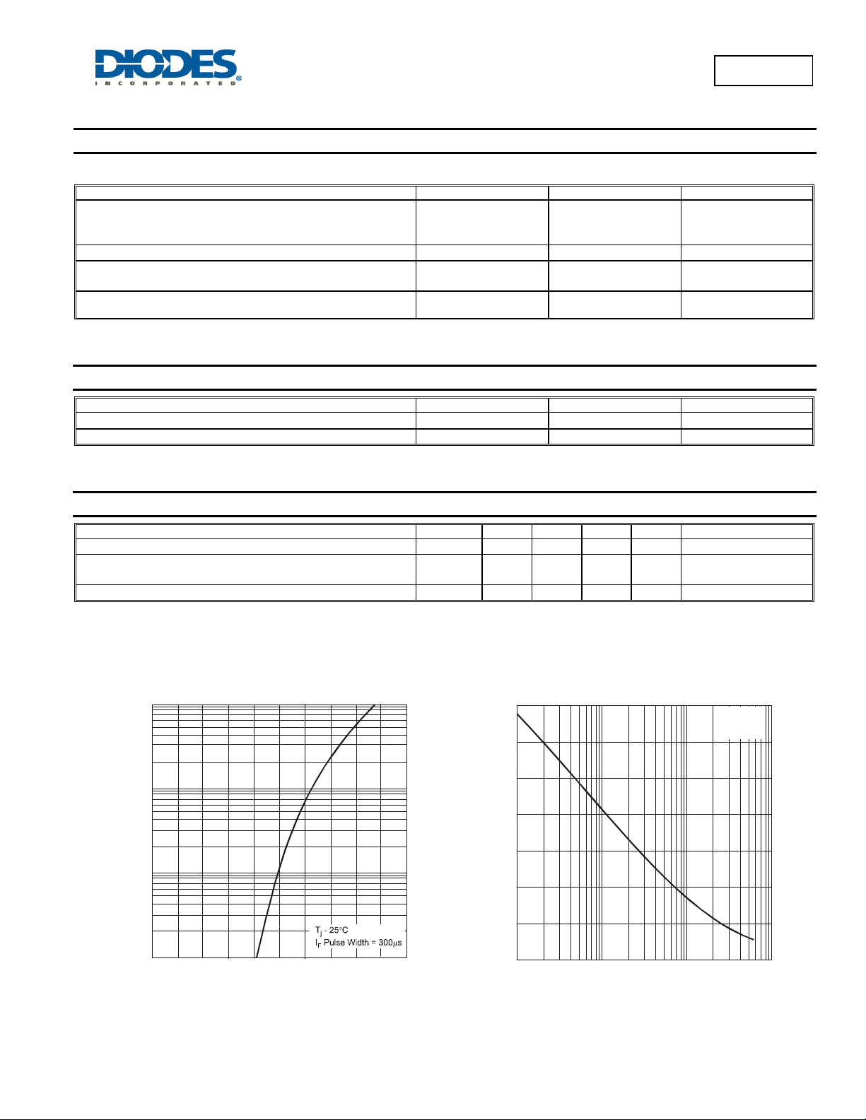
IF = 1.0A, TA = 25°C
= 100V, TA = 25°C
V
R
= 100V, TA = 100°C
V
R
VR = 4V, f = 1MHz
f = 1.0MHz
°
T = 25C
j
A
160
A
120
AL (p
80
,
T
40
F
I , INS
0.01
0 0.2 0.4 0.6 0.8 1.0
V , INSTANTANEOUS FORWARD VOL TAGE (V)
F
Fig. 1 Typical Forward Characteristics
0
10.1 10 100
V , DC (V)
REVERSE VOLTAGE
R
Fig. 2 T otal Capacitance vs. Reverse Voltage
B1100LB
Document number: DS30077 Rev. 10 - 2
2 of 4
www.diodes.com
September 2010
© Diodes Incorporated
Page 3

RAGE FORWARD CUR
R
N
T
P
FORWAR
U
R
GE CUR
RENT
4
(A)
E
3
2
1
F(AV),
I AVE
0
25 50 75 100 125 175
T , TERMINAL TEMPERA TURE ( C)
T
Fig. 3 Forward Current Derating Curve
150
°
50
(A)
40
30
D S
20
10
EAK
FSM
I,
0
110100
Fig. 4 Max Non-Repetitive Peak Forward Surge Current
NUMBER OF CYCLES AT 60Hz
B1100LB
Package Outline Dimensions
A
J
B
SMB
Dim Min Max
C
D
G
H
A 3.30 3.94
B 4.06 4.57
C 1.96 2.21
D 0.15 0.31
E 5.00 5.59
G 0.05 0.20
H 0.76 1.52
J 2.00 2.50
All Dimensions in mm
E
Suggested Pad Layout
B1100LB
Document number: DS30077 Rev. 10 - 2
3 of 4
www.diodes.com
Dimensions Value (in mm)
Z 6.8
G 1.8
X 2.3
Y 2.5
C 4.3
September 2010
© Diodes Incorporated
Page 4

IMPORTANT NOTICE
DIODES INCORPORATED MAKES NO WARRANTY OF ANY KIND, EXPRESS OR IMPLIED, WITH REGARDS TO THIS DOCUMENT,
INCLUDING, BUT NOT LIMITED TO, THE IMPLIED WARRANTIES OF MERCHANTABILITY AND FITNESS FOR A PARTICULAR PURPOSE
(AND THEIR EQUIVALENTS UNDER THE LAWS OF ANY JURISDICTION).
Diodes Incorporated and its subsidiaries reserve the right to make modifications, enhancements, improvements, corrections or other changes
without further notice to this document and any product described herein. Diodes Incorporated does not assume any liability arising out of the
application or use of this document or any product described herein; neither does Diodes Incorporated convey any license under its patent or
trademark rights, nor the rights of others. Any Customer or user of this document or products described herein in such applications shall assume
all risks of such use and will agree to hold Diodes Incorporated and all the companies whose products are represented on Diodes Incorporated
website, harmless against all damages.
Diodes Incorporated does not warrant or accept any liability whatsoever in respect of any products purchased through unauthorized sales channel.
Should Customers purchase or use Diodes Incorporated products for any unintended or unauthorize d application, Customers shall indemnify and
hold Diodes Incorporated and its representatives harmless against all claims, damages, expenses, and attorney fees arising out of, directly or
indirectly, any claim of personal injury or death associated with such unintended or unauthorized application.
Products described herein may be covered by one or more United States, international or foreign patents pending. Product names and markings
noted herein may also be covered by one or more United States, international or foreign trademarks.
LIFE SUPPORT
Diodes Incorporated products are specifically not authorized for use as critical components in life support devices or systems without the express
written approval of the Chief Executive Officer of Diodes Incorporated. As used herein:
A. Life support devices or systems are devices or systems which:
1. are intended to implant into the body, or
2. support or sustain life and whose failure to perform when properly used in accordance with instructions for use provided in the
labeling can be reasonably expected to result in significant injury to the user.
B. A critical component is any component in a life support device or system whose failure to perform can be reasonably expected to cause the
failure of the life support device or to affect its safety or effectiveness.
Customers represent that they have all necessary expertise in the safety and regulatory ramifications of their life support devices or systems, and
acknowledge and agree that they are solely responsible for all legal, regulatory and safety-related requirements concerning their products and any
use of Diodes Incorporated products in such safety-critical, life support devices or systems, notwithstanding any devices- or systems-related
information or support that may be provided by Diodes Incorporated. Further, Customers must fully indemnify Diodes Incorporated and its
representatives against any damages arising out of the use of Diodes Incorporated products in such safety-critical, life support devices or systems.
Copyright © 2010, Diodes Incorporated
www.diodes.com
B1100LB
B1100LB
Document number: DS30077 Rev. 10 - 2
4 of 4
www.diodes.com
September 2010
© Diodes Incorporated
 Loading...