

Page 1
)
θ
θ
(BR)
Please click here to visit our online spice models database.
Features
• Low Forward Voltage Drop
• Guard Ring Construction for Transient Protection
• High Conductance
• Lead, Halogen and Antimony Free, RoHS Compliant (Note 1)
• "Green" Device (Note 5)
• Qualified to AEC-Q101 Standards for High Reliability
Maximum Ratings @T
Single phase, half wave, 60Hz, resistive or inductive load.
For capacitance load, derate current by 20%.
Peak Repetitive Reverse Voltage
Working Peak Reverse Voltage
DC Blocking Voltage
RMS Reverse Voltage
Average Rectified Output Current (See Figure 4)
Non-Repetitive Peak Forward Surge Current
8.3ms single half sine-wave superimposed on rated load
= 25°C unless otherwise specified
A
Characteristic Symbol Value Unit
B0540W
0.5A SURFACE MOUNT SCHOTTKY BARRIER RECTIFIER
Mechanical Data
• Case: SOD-123
• Case Material: Molded Plastic, “Green” Molding Compound
(Note 5). UL Flammability Classification Rating 94V-0
• Moisture Sensitivity: Level 1 per J-STD-020D
• Lead Free Plating (Matte Tin Finish annealed over Alloy 42
leadframe) Solderable per MIL-STD-202, Method 208
• Polarity: Cathode Band
• Marking Information: See Page 3
• Ordering Information: See Page 3
• Weight: 0.01 grams (approximate)
Top View
V
V
V
R(RMS
I
RRM
RWM
VR
IO
FSM
40 V
28 V
0.5 A
5.5 A
Thermal Characteristics
Characteristic Symbol Typ Max Unit
Thermal Resistance Junction to Ambient Air (Note 2) TA = 25°C
Thermal Resistance Junction to Ambient Air (Note 3) TA = 25°C
Operating and Storage Temperature Range
Electrical Characteristics @T
Characteristic Symbol Value Unit Test Conditions
Minimum Reverse Breakdown Voltage (Note 4)
Maximum Forward Voltage Drop
Maximum Leakage Current (Note 4)
Total Capacitance
Notes: 1. No purposefully added lead. Halogen and Antimony Free.
V9 are built with Non-Green Molding Compound and may contain Halogens or Sb
B0540W
Document number: DS30138 Rev. 10 - 2
2. FR-4 PCB, minimum recommended pad layout per http://www.diodes.com/datasheets/ap02001.pdf.
3. Polymide PCB, minimum recommended pad layout per http://www.diodes.com/datasheets/ap02001.pdf.
4. Short duration pulse test used to minimize self-heating effect.
5. Product manufactured with Data Code V9 (week 33, 2008) and newer are built with Green Molding Compound. Product manufactured prior to Date Code
A
R
JA
R
JA
TJ, T
= 25°C unless otherwise specified
V
VFM
IRM
CT
1 of 3
www.diodes.com
STG
R
Fire Retardants.
2O3
385
325
-65 to +150 °C
40 V
0.510
0.620
0.460
0.610
10
20
5.0
13
170 pF
⎯
⎯
IR = 20μA
IF = 0.5A, TJ = 25°C
IF = 1.0A, TJ = 25°C
V
IF = 0.5A, TJ = 100°C
IF = 1.0A, TJ = 100°C
VR = 20V, TJ = 25°C
μA
VR = 40V, TJ = 25°C
VR = 20V, TJ = 100°C
mA
VR = 40V, TJ = 100°C
f = 1MHz, VR = 0V DC
°C/W
°C/W
March 2009
© Diodes Incorporated
Page 2
P
P
OWER
P
TIO
C, TOT
CAPACITAN
C
F
RAG
F
O
R
RD CUR
R
N
T
B0540W
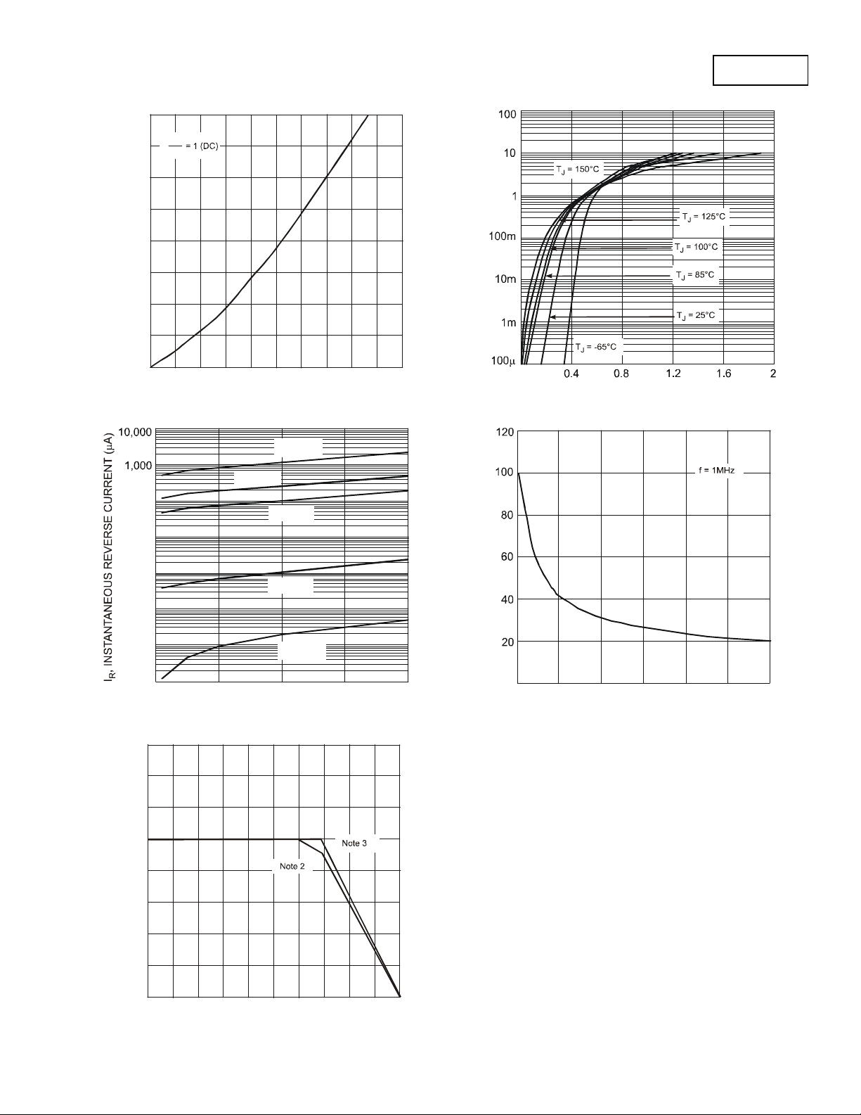
0.4
I
PK
I
AV
0.3
N (W)
A
0.2
DISSI
,
0.1
D
F
0
00.1
I , AVERAGE FORWARD CURRENT (A)
F(AV)
0.4
0.30.2
0.5 0.6 0.7 0.8
Fig. 1 Forward Power Dissipation
T = 125°C
J
0.9
1
I , INSTANT ANEOUS FORWARD CURRENT (A)
0
V , INSTANTANEOUS F O RW ARD VO LT AGE (V )
F
Fig. 2 Typical Forward C haracter istics
(A)
E
WA
T = 100°C
J
100
T = 85°C
J
10
1
T = 25°C
J
0.1
0.01
T = -65°C
J
0.001
0
V , INSTANTANEOUS REVERSE VOLTAGE (V)
R
10
20
Fig. 3 Typical Reverse Characteristics
0.8
0.7
0.6
0.5
0.4
30
40
)
E (p
AL
T
0
01020
V , DC REVERSE VOLTAGE (V)
R
Fig. 4 T otal Capacitance vs. Reverse Voltage
25
30515
E
0.3
0.2
0.1
F(AV)
I, AVE
0
03060
T , AMBIENT TEMPERATURE (°C)
A
90
120
150
Fig. 5 Forward Current Derating Curve
B0540W
Document number: DS30138 Rev. 10 - 2
2 of 3
www.diodes.com
March 2009
© Diodes Incorporated
Page 3

B0540W
Ordering Information (Note 6)
Part Number Case Packaging
B0540W-7-F SOD-123 3000/Tape & Reel
Notes: 6. For packaging details, go to our website at http://www.diodes.com/datasheets/ap02007.pdf.
Marking Information
Date Code Key
Year 1998 1999 2000 2001 2002 2003 2004 2005 2006 2007 2008 2009 2010 2011 2012
Code J K L M N P R S T U V W X Y Z
Month Jan Feb Mar Apr May Jun Jul Aug Sep Oct Nov Dec
Code 1 2 3 4 5 6 7 8 9 O N D
SF
SF = Product Type Marking Code
YM = Date Code Marking
Y = Year (ex: N = 2002)
YM
M = Month (ex: 9 = September)
Package Outline Dimensions
B
M
C
H
SOD-123
A
K
L
Dim Min Max
A 0.55 Typ
B 1.40 1.70
C 3.55 3.85
H 2.55 2.85
J 0.00 0.10
K 1.00 1.35
L 0.25 0.40
M 0.10 0.15
α
All Dimensions in mm
0 8°
Suggested Pad Layout
Diodes Incorporated and its subsidiaries reserve the right to make modifications, enhancements, improvements, corrections or other changes
without further notice to any product herein. Diodes Incorporated does not assume any liability arising out of the application or use of any product
described herein; neither does it convey any license under its patent rights, nor the rights of others. The user of products in such applications shall
assume all risks of such use and will agree to hold Diodes Incorporated and all the companies whose products are represented on our website,
harmless against all damages.
Diodes Incorporated products are not authorized for use as critical components in life support devices or systems without the expressed written
approval of the President of Diodes Incorporated.
X
Y
B0540W
Document number: DS30138 Rev. 10 - 2
C
G
Z
IMPORTANT NOTICE
LIFE SUPPORT
3 of 3
www.diodes.com
Dimensions Value (in mm)
Z 4.9
G 2.5
X 0.7
Y 1.2
C 3.7
March 2009
© Diodes Incorporated
 Loading...